PCB Stack-Up Matching to Select Design and Optimize Materials
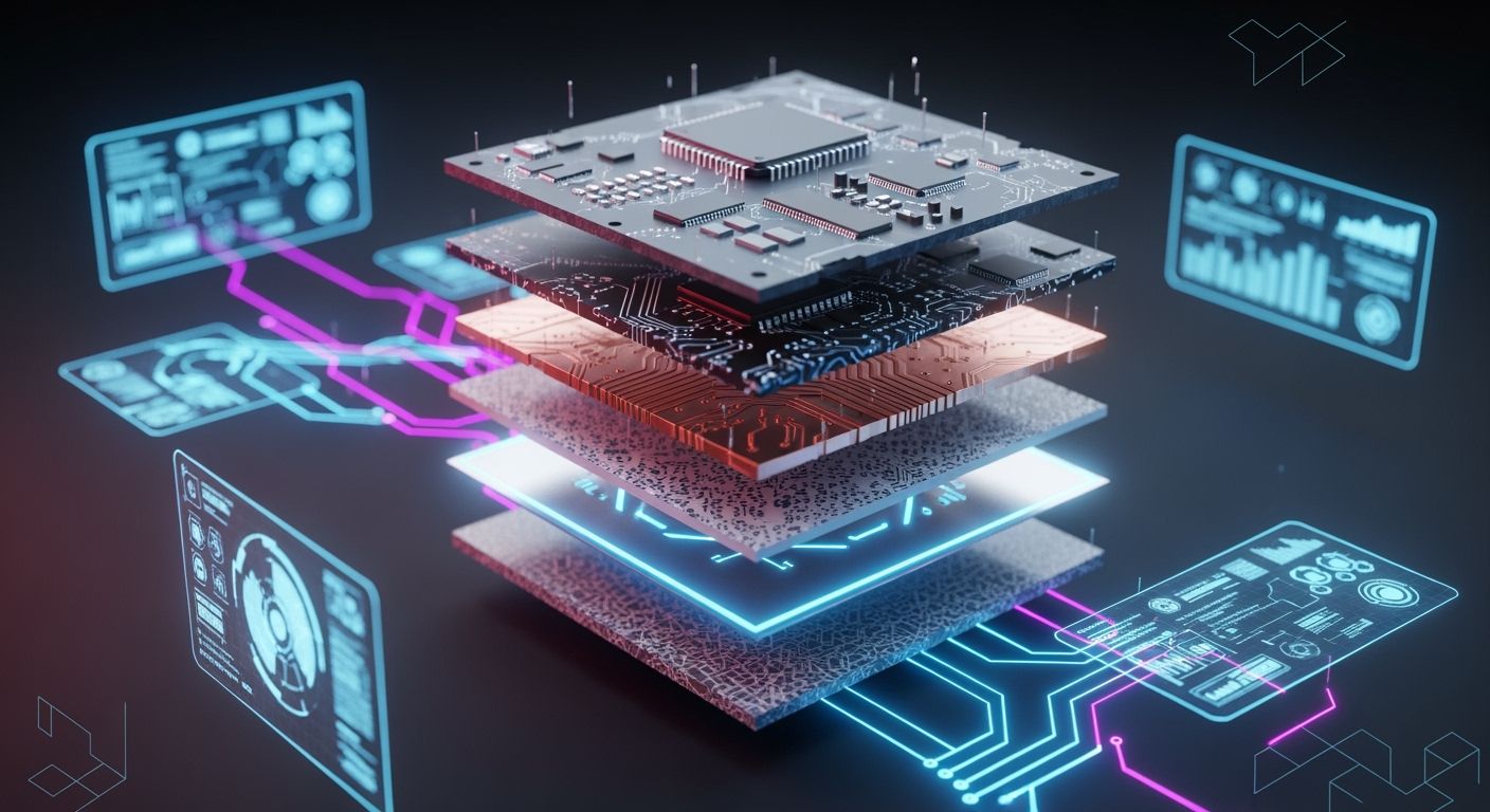
Good PCB stack-up matching requires careful planning. You must align core materials first. You must align prepreg layers next. Also, check dielectric thicknesses and layer order. Do this before starting layout.
You can map electrical parameters now. Map parameters like Dk and Df. Also map thermal properties like Tg. Include CTE properties for your target layers. Use a structured pcb material selection framework.
Target Parameter | Key Properties | Structural Elements |
|---|---|---|
Electrical Integrity | Dk / Df | Core & Prepreg Thickness |
Thermal Stability | Tg / CTE | Layer Balance & Copper Weight |
Early stack-up design stops signal loss. It controls board warpage very well. It also prevents performance drops over time. Define your stack-up very early on. This ensures total PCB Material Compatibility always. It improves printed circuit board materials greatly. This helps high-frequency signal reliability succeed.
Key Takeaways
Plan your PCB stack-up early to prevent signal loss and stop board warpage.
Match material expansion rates to protect tiny copper vias from heat damage.
Mirror copper layers around the center to keep circuit boards flat and strong.
Work with your board maker early to improve factory output and cut costs.
PCB Material Compatibility and Standards
Engineers must meet tough rules. They build complex circuit boards. They match core laminates well. They select proper prepregs, too. This stops field failures. Ideal materials ensure stable performance. They work in extreme heat.
Substrate Electrical Parameters: Dk and Df
Dielectric constant (Dk) affects signal speed. Signals travel on copper traces. Dissipation factor (Df) measures power loss. Loss happens in the dielectric. High frequencies exceed 10 GHz. Poor substrate materials lose energy. Energy drops very fast. You need stable materials. They save your timing margins.
Dielectric Parameter | Material Value / Example | Frequency / Conditions | Signal Loss & Performance Impact |
|---|---|---|---|
Loss Tangent (Df) | High Df (0.01 – 0.02) | 10 GHz | Signals turn into heat fast. Heat causes severe signal loss. Long traces suffer data errors. |
Loss Tangent (Df) | Low Df (0.001 – 0.003) | 10 GHz (Advanced Laminates) | Energy loss stays very low. Signals do not degrade much. Communication links stay very reliable. |
Loss Tangent (Df) | Ultra-Low Df (0.0003) | 10 GHz (PTFE Material) | Energy loss stays minimal. Heat generation remains low. It fits RF and microwave. |
Dielectric Constant (Dk) | Lower Dk (2.1 – 2.2 vs. 4.4) | High Frequency (≥ 10 Gbps) | Lower values boost signal speed. Signal delays decrease quickly. Stable impedance stops power reflections. |
Lower Dk values boost speed. High-speed lines move faster. Keep Dk uniform everywhere. This protects total system integrity.
Thermal and Mechanical Metrics: Tg, Td, and CTE
Heat changes board shape directly. You must monitor mechanical limits. This protects delicate copper vias. Do this during assembly.
Peak Thermal Exposure: Lead-free reflow uses SAC305. Temps reach 245–260°C. That is far above FR4 Tg. Normal Tg is 130–140°C.
Dimensional Degradation: Soft resin shifts inner layers. Multilayer boards shift internally. This causes registration errors. Vias miss pads completely.
Thermal Degradation Rate: Polymer breakdown speeds up fast. It doubles every 10°C. This happens past Tg.
Td Margin Safety: High Td laminates reach 340°C. High values add safe margins. They prevent permanent heat damage. Hot profiles cause damage.
The table shows physical shifts. It explains structural impacts:
Parameter | Physical/Chemical Impact | Reliability Consequences in Lead-Free Reflow |
|---|---|---|
Glass Transition Temp (Tg) | - Hard boards turn rubbery. | - Higher Coefficient of Thermal Expansion (CTE). |
Decomposition Temp (Td) | - Chemical bonds break down. | - Damage becomes total failure. |
Match the Coefficient of Thermal Expansion (CTE). Balance X, Y, Z axes. This maintains solid board structure. Z-axis growth strains plated vias. High-Tg laminates stop cracked vias. High-Td materials help, too. Use them in stack-up design.
Copper Foil Profiles and Surface Roughness
Smooth copper reduces conductor loss. High frequencies create skin effect. Currents flow near outer skin. Standard electrodeposited (STD) copper stays rough. Rough surfaces form longer paths. They weaken fast signals.
Use Very Low Profile (VLP) copper. Hyper Very Low Profile (HVLP) works. Smooth profiles fix phase distortion. High-speed digital links run better. Smooth foil helps pcb material compatibility. Peel strength stays very strong.
IPC-4101 and IPC-4103 Material Standards
IPC-4101 standards list fiberglass epoxy. They now support lead-free work. They fit RoHS rules well. They suit standard rigid boards. IPC-4103 covers clad plastic laminates. It includes unclad plastics, too. It adds bondply materials. High-speed PCB setups need these.
Technical Dimension | IPC-4101 Standard | IPC-4103 Standard |
|---|---|---|
Primary Scope | Rigid base circuit materials | Base materials for high speeds |
Material Characteristics | Standard laminates and prepregs | Advanced plastics with low loss |
Target Applications | Common rigid circuit boards | Stripline and microwave circuits |
Core Control Focus | Grading and sheet thickness | Accurate dielectric constant (Dk) controls |
Pick right slash sheets carefully. High-reliability systems need them. These IPC-4101 slash numbers fit:
IPC-4101/99
IPC-4101/101
IPC-4101/126
These rules set high Td. They limit Z-axis CTE expansion. Good materials simplify stackups now. They boost pcb manufacturing yield. Matching materials ensures great durability. Complex stackups last much longer. Early pcb material compatibility stops redesigns.
PCB Stack-Up Architecture for Signal Integrity
Plan your stack-up carefully. Good planning protects signal integrity. It keeps boards stable. Control plane symmetry. Use solid reference planes. This gets top results.
Layer Symmetry and Stack-Up Balance
Symmetrical designs prevent warping. Balance materials around the middle.
Uneven layer designs cause stress. Light lines oppose heavy copper. Heat and pressure hurt them. Unbalanced forces bend boards. Unbalanced boards bend and twist.
Key Rule for Physical Balance: Mirror copper weights and layers.
Watch out for these risks:
Unbalanced Heat: Unequal layers cause uneven expansion. Lamination heat strains the board.
Unequal Copper Weight: Different copper weights cause uneven cooling.
Unbalanced Prepreg: Uneven prepreg alters resin flow.
Heavy Copper Placement: Thick outer copper increases heat stress.
Smart stack-ups protect board structures. Careful planning ensures long life.
Reference Plane Coupling and Return Paths
Fast signals need return paths. Put signal lines near ground.
Placing signals near planes lowers height. It reduces loop inductance. Return currents stay under traces. Small loop areas lower noise.
Never cross split planes. Splits damage signals three ways:
Direct Noise Increase: Crossing gaps creates clear noise.
Mode Conversion and Skew Effects: Timing gaps create common noise. Noise increases with gap size.
Radiation Mechanism: Plane gaps act like antennas. Antennas radiate bad interference.
Keep reference planes solid. Solid planes protect fast signals.
Impedance Control for Differential Pairs
Fast buses need strict impedance control. Calculate trace sizes before routing.
Parameter | Target Specification | Impact on Signal Integrity |
|---|---|---|
Single-Ended Impedance | 50 Ohms ± 10% | Prevents signal reflections |
Differential Impedance | 90 - 100 Ohms ± 10% | Maintains differential signal balance |
Trace Spacing | 3x Dielectric Height | Achieves effective crosstalk reduction |
Good stack-ups ease impedance control. Adjust trace sizes to stop distortion. Keep pairs close together.
  [ Trace 1 ]    [ Trace 2 ]   <-- Differential Pair
======= Dielectric Material =======
----------------------------------- <-- Solid Reference Plane
Good spacing prevents crosstalk. Isolate lines to stop noise. Clean lines save data.
Power Plane Placement and Decoupling
Put power and ground together. Thin layers add high capacitance.
Place power next to ground. Close spacing lowers high-frequency impedance. Fast chips draw power quickly.
Short vias to capacitors help. Every board needs low inductance.
Good stack-ups deliver clean power. Smart layouts protect sensitive signals.
Advanced Stack-Up Design for Hybrid and HDI Boards
New circuit boards need fresh materials. They also need smart building steps. You can mix different materials. This helps save money. It also boosts board performance.
Hybrid Stack-Ups: High-Speed and FR-4
You can mix FR-4 layers. Use them with high-speed PTFE layers. High-speed systems need special laminates. Put them on outer layers. This keeps signal loss low. Follow these rules to stop peeling:
Thermal Expansion Management: Match the CTE values. This reduces stress at layer seams.
Bonding Control: Use correct pressure during press. Strong pressure holds different materials together.
Fabrication Practices: Use specialized build steps. Careful steps stop board warping later.
Resin Content and Prepreg Flow Calculation
Calculate resin fill needs early on. Standard prepreg holds resin and glass. Heat melts this resin. The liquid fills copper gaps.
Too little resin creates air gaps. Too much resin makes layers uneven. Pick exact resin amounts carefully. This keeps dielectric thickness steady everywhere. Steady layers protect fast signals.
HDI, Microvias, and Sequential Lamination
HDI designs use tiny microvias. You use sequential lamination here. This builds small boards step-by-step.
Important HDI Rule: Keep layers balanced around core. Equal press runs prevent trace damage.
Microvias save a lot of space. Small vias allow tighter trace routing. You can place parts closer now. This also stops bad crosstalk.
Glass Weave Selection and Fiber-Weave Effect
Regular glass weaves have gaps. Traces pass over glass and resin. This shift changes signal speed. It creates timing errors fast. Spread-glass flattens these glass fibers. This removes open gaps completely.
Parameter / Property | Standard Glass Weaves (e.g., 106, 1080) | Spread / Flat Glass Weaves (e.g., 1067, 1078) |
|---|---|---|
Physical Structure | Open gaps between yarn bundles | Flat glass fibers with no gaps |
Dielectric Environment | Changing Dk shifts signal speed | Flat Dk keeps signal speed steady |
Impact on Timing Skew | Causes timing errors on lines | Fixes timing errors in fast designs |
Choose spread glass for better boards. It offers a smooth dielectric layer. You can also turn traces slightly. Angled lines cross glass evenly. This easy step stops timing errors. It also cuts bad crosstalk.
A good stackup protects total system health. Talk to your maker early on. Check every layer with them. Good plans keep signals steady. You build top boards this way.
Thermal and Mechanical Stack-Up Stability
Heat strains circuit boards during production and operation. Manage heat to keep boards strong. Smart choices protect your builds.
Z-Axis CTE Mismatch and Plated Through-Hole Reliability
Heat makes board parts expand differently. Fibers stop side expansion. Unheld resin grows thick very fast.
Axis | CTE Rate (ppm/°C) | Structural Constraint | Impact on PTH Integrity |
|---|---|---|---|
X-Y Axis | 14–17 | High (constrained by glass fibers) | Minimal dimensional change |
Z-Axis | 50–70 (increases above Tg) | Low (unconstrained through thickness) | Concentrates intense stress on barrel walls and interlayer bonds |
Heat ruins inner copper in four steps:
Reflow Heating Above Tg: Reflow heat hits 260°C. That heat beats normal Tg.
Resin Softening & Z-Axis Expansion: Soft resin expands along Z-axes quickly.
Plating Stress: Thick boards push hard on copper walls.
Failure Occurrence: High stress cracks thin copper walls.
Pick high-Tg materials for thick boards.
Warpage Prevention During Reflow Soldering
Uneven heat bends hot boards badly. Balance middle copper weights for flat boards. IPC-6012 limits board bending to 0.75%. Symmetrical layers keep boards flat always.
Microvia Reliability in High-Density Designs
Dense designs stress tiny microvias hard. Staggered microvias increase total board strength.
Copper-Dielectric Interface Cracking: Thermal growth pushes copper walls outward. Cracks widen during heat cycles.
Fill Voiding and Resin Pumping: Hot epoxy swells inside microvias. Swelling weakens copper barrels.
Compounded Stacked Vulnerability: Stacked vias concentrate Z-axis stress. Repeated heat causes open circuits.
Staggered Reliability Advantage: Staggering spreads stress across layers. Offset vias follow IPC-2226 rules.
Microvia Configuration | Thermal Stress Behavior | Specific Failure Mechanisms |
|---|---|---|
Stacked Microvias | Creates a solid copper column that concentrates 100% of shear and axial stress at a single point during z-axis laminate expansion (~200 ppm/°C vs. ~16 ppm/°C for copper). | • Interfacial separation (breaking bond between stacked vias) |
Staggered Microvias | Offsets layers across different z-axis planes, utilizing the dielectric material as a shock absorber to distribute thermal loads stepwise. | Demonstrates superior fatigue resistance with failure rates below 0.5% over 400 thermal shock cycles, mitigating weak interface separations. |
Offset microvias stop heat damage early. This choice secures all your connections.
Thermal Dissipation Vias and Metallic Cores
Hot chips create severe local heat. Route heat away using special paths.
Thermal Via Arrays: A 6x6 via grid cools chips. Junction heat drops by 4.8°C. Filled vias drop heat resistance 20%.
Metal Core Substrates (MCPCBs): Metal cores move heat faster. Aluminum works better than FR-4. Rapid cooling stops chip damage.
Good heat plans boost total performance. Match materials to protect board builds. Smart stack-ups help hardware last long.
Material Optimization and Stack-Up Matching Matrix
Smart choices cut overall board costs. They also boost signal speed fast. Select optimal pcb material choices carefully now. This balances electrical needs with factory skills.
Performance versus Cost Trade-Off Analysis
Smart stack-ups prevent costly over-engineering. Great laminates boost high-frequency signal delivery well. Cheap FR-4 layers cut costs on power. Put top substrates where signals need them.
Pro Tip: Match material grade to circuit speed directly. This boosts overall performance without adding costs.
Good stack-ups balance electrical safety with tight budgets. You keep thermal performance and product durability safe.
Standardizing Dielectric and Prepreg Thicknesses
Standard glass styles make stack-ups easy to build. Single prepregs measure 0.002 to 0.010 inches thick. Fast signals need thin dielectric layers. Keep them between 0.003 and 0.005 inches. This holds tight impedance control.
Glass Style | Thickness Spec (mm) | Resin Ratio |
|---|---|---|
Style 106 | 0.05 | ~73% |
Style 1080 | 0.075 | ~65% |
Style 3313 | 0.09 | ~57% |
Style 2116 | 0.115 | ~55% |
Style 7628 | 0.185 | ~46% |
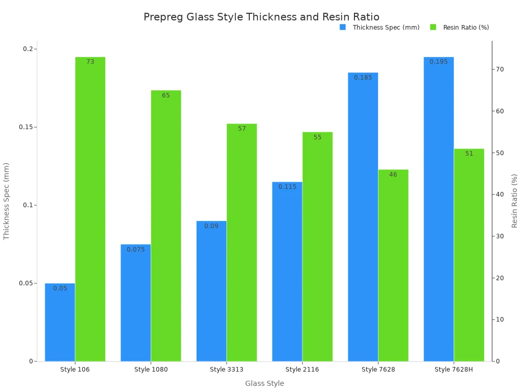
Standard glass weaves speed up panel press steps. Accurate dielectric choices ensure total pcb material compatibility.
Fabricator DFM Rules and Stack-Up Verification
Check custom stack-ups with your factory first. Do this before routing traces. Early checks prevent costly factory delays now. They also stop board bending.
Check exact pcb stack-up balance with makers.
Review resin fill needs for heavy copper.
Check final board thickness against case limits.
Makers adjust copper thickness during press steps. Early reviews align stack-ups with real factory limits. Proper stack-ups bring high factory yields and stability.
Matching board materials to your stack-up keeps signals clear. It also keeps the board strong. You must keep layers equal on both sides. Also, match thermal expansion rates. Pick exact Dk/Df grades to stop signal loss. Always check resin levels to protect performance.
A balanced stack-up improves your design layout. Talk to board makers early in design. Checking your stack-up early locks in details. It also raises factory output.
FAQ
How do you maintain signal integrity in high-speed applications?
Match trace sizes to target impedance. Place solid ground planes near routing layers. Pick low-loss dielectric substrates for fast designs. These steps keep signals clear and strong. They also stop energy loss effectively.
Why does pcb material compatibility matter for stack-up design?
Good pcb material compatibility stops structural board failures. Match thermal expansion rates across different layers. This step stops severe peeling and warping. It also keeps your circuit board stable. Boards stay safe during reflow soldering.
When should you select specialized high-speed laminates?
Pick high-speed laminates when data exceeds gigabit speeds. Standard FR-4 materials absorb too much signal energy. They lose power at high frequencies. High-speed core layers keep signals clear. They also boost total circuit performance.
See Also
A Complete Guide To Essential HDI Multilayer PCB Stackups
Best Practices For Designing High Performance LED Circuit Boards
Evaluating Cost And Benefits Of Advanced HDI Microvia Structures
Solving Common SMT PCB Design Issues For Better Manufacturing
