High-Speed PCB vs Ordinary PCB: Core Differences
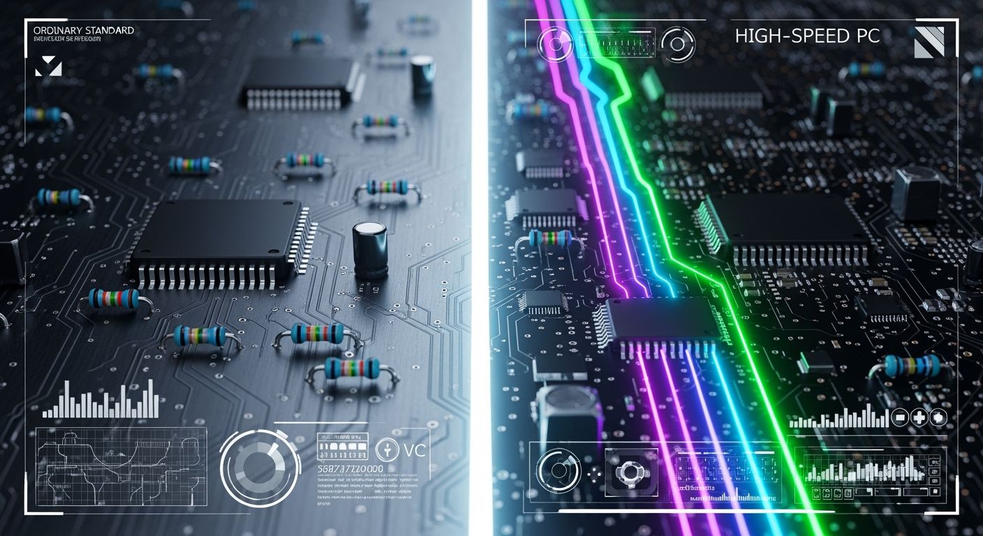
Engineers often group PCB abilities by their operating clock speed. However, fast signal changes and rise times under 1ns show you are dealing with a real high-speed digital PCB. A standard PCB serves as a simple base that holds basic electrical connections together. In contrast, a high-speed PCB works like a dynamic transmission line part inside your system. You have to protect signal quality and control impedance on every line that runs at top speeds. Making bad layout choices quickly lowers total system performance and ruins signal clarity. Because of this, you must keep signal quality high and maintain fast bus speeds. You compare Core Differences by looking at dielectric material choices, exact manufacturing limits, special PCB layout rules, and total design quality in tough real-world uses.
Key Takeaways
How fast a signal changes matters more than clock speed for high-speed boards.
Solid, continuous ground planes stop signals from weakening and keep out unwanted interference.
High-quality board materials like Rogers 4350B lower heat generation and prevent signal loss.
Strict factory rules ensure clean signal movement through every layer.
Core Differences in PCB Design
You need to check two main changes when switching from normal board design styles. On a basic board, copper lines act like simple wires that carry power. But on a fast digital board, every track acts as an active signal path. You cannot view traces as simple wire paths. Instead, you must carefully control signal timing, speed changes, and travel delays across your board.
Transmission Line Behavior
You must treat trace paths like active parts when managing fast digital signals. Signal energy moves through the board material rather than just the copper lines. Because of this, signal movement depends on solid metal reference layers. You must place unbroken copper layers right below your lines to stop signal path breaks.
"The return current of a high-speed, fast-rise time digital signal will always follow the path of least inductance, which is directly beneath the signal path. However, discontinuities tend to divert the return current, increasing the loop area, inductance, and delay... Without a proper return path layout, you might find yourself with currents spreading around splits in your ground plane, leading to a loss of signal integrity."
You must use exact line paths to stop signal bouncing and power loss. You should route paired signal lines on the exact same layer to keep conditions even. You must avoid putting extra parts or holes between lines because extra items cause energy bumps and noise. Fast board layouts require careful line length matching across all parts to keep signals moving together. Also, you must use fewer layer holes because every hole adds unwanted resistance.
Design Aspect | High-Speed PCB Approach | Ordinary PCB Approach |
|---|---|---|
Impedance Control Priority | Careful attention is required to keep signals clean at high speed levels. | Usually fine to just reduce extra noise, mostly to pass safety tests. |
Reference Plane Continuity | Needs an unbroken copper layer directly under the signal line. | Less important; lines can handle larger breaks in the metal layer. |
Signal Frequency vs Edge Rate
People often link board performance to clock speed alone, but signal rise speed controls real board actions. A quick signal jump expands the working frequency range no matter the main clock speed. You can find the top frequency using the math formula speed = 0.35 / rise time. A slow 10 ns rise time needs a lower 35 MHz frequency range. By comparison, a fast 1 ns rise time needs a higher 350 MHz range to keep signal shapes clean without extra loss.
You check critical line length to learn when signal effects take over a circuit board. You can use the formula L_critical = (Rise Time) / (2 × Propagation Delay per unit length). For standard FR-4 board materials with a delay of 147 ps/inch, a 0.5 ns rise time gives a main length of 1.7 inches. When delay passes 20% of the rise time, long-line signal behavior begins. For example, a 1 ns rise time moving at 6 inches per nanosecond sets a limit at 1.2 inches.
You must change your board setup plan when working with very fast signal paths. For signals running faster than 1 GHz, length gaps inside line pairs must stay below 1 inch. Using strict rules for fast digital design stops timing mistakes across all your quick signals. Placing extra ground holes near signal paths keeps power flowing smoothly. These key changes turn basic board design work into expert high-speed board engineering, keeping circuits fast and systems running well across high-speed lines.
High-Speed PCB Signal Integrity
Controlled Impedance Rules
You must guard high-speed signal integrity across all pcb layers during production. Mismatched impedance damages trace integrity, creating unwanted signal reflections. Basic PCB design guidelines follow IPC-2221 baseline stackup parameters and IPC standards. Even so, complex high-speed designs need specialized rules. You can check IPC-2141A for detailed formulas about microstrip structures. Exact routing geometry stops trace degradation while keeping signal integrity strong.
IPC Standard | Description |
|---|---|
IPC-2141A | Design Guide for High-Speed Controlled Impedance Circuit Boards. |
IPC-2221C | Generic Standard on Printed Board Design. |
High-speed digital signals need exact dielectric constant values from IPC-4101 standards. Choosing the right material cuts energy loss while signals move. Target values like differential return loss below -10 dB up to the Nyquist frequency protect waveform quality. Smart high-speed signal routing helps you get return loss below -15 dB at via transitions. Clever trace paths protect pcb power integrity. Exact trace parameters stop signal distortion across your pcb layout.
Crosstalk and EMI Control
High-speed signal routing uses strict trace spacing rules to block noise. Trace routing directly impacts signal clarity on every pcb path. Setting traces far apart stops unwanted coupling from parasitic capacitance. You must shield critical paths across your high-speed digital pcb layout. Keeping wide gaps stops crosstalk, preserves system integrity, and protects signal quality. Solid ground layers keep return paths small and low in inductance to save data integrity.
The highest-frequency signal on your board determines your EMI shielding requirements. Remember that a 100 MHz square wave contains significant energy at its 5th, 7th, and 9th harmonics (500 MHz, 700 MHz, 900 MHz), so shield for the harmonic content, not just the fundamental.
Every high-speed pcb requires strong electromagnetic interference protection. High-speed digital signals throw off heavy radiation at harmonic frequencies. You can put via stitching near board edges to trap stray fields inside the pcb. Metal shield cans protect sensitive components on the pcb. Following strict high-speed digital design rules ensures full compliance with industry standards. Modern high-speed designs keep strong integrity across all high-speed digital pcb layers.
Material Selection for Speed
Choosing the right PCB material directly changes board speed and performance. You need board materials that manage super fast data streams without losing signal quality.
Dk and Df Performance Metrics
Dielectric constant (Dk) controls how fast signals travel through every board line. The math equation v = c / √Dk shows that signal speed drops when Dk goes up. A lower Dk makes signals move faster while cutting travel delays. You need low Dk values in network gear, AI servers, and data centers. Quick signals need precise material setup to keep all timing aligned.
Dk defines how much the material slows down an electric signal compared to the speed of light in a vacuum. Higher Dk slows signal propagation.
Dissipation factor (Df) measures energy loss along your board trace lines. A higher Df causes heavy signal loss and unwanted heat. Running at high frequencies multiplies this loss rate by a lot. Choosing low-loss materials stops total signal fading at high speeds. Lower loss keeps signal edges sharp and protects the overall wave shape.
Standard FR-4 vs Advanced Substrates
Standard FR-4 offers cheap base material choices for basic designs. But standard FR-4 shows a high Dk of 4.20 and a high Df of 0.028 at 10 GHz. This high loss creates bad signal drop during high-speed runs. Tech reference data shows that FR-4 causes heavy dielectric loss when speed goes up. You must upgrade your board setup to stop extra signal loss.
Advanced low-loss materials replace standard FR-4 on tough high-speed designs. Special low-loss materials keep Dk steady and Df low across wide working ranges. Smart material choices balance production costs with your target speed goals. You reduce overall board power loss by picking higher grade material options. Picking better board materials improves total circuit operation.
Material | Dk (Dielectric Constant) at 10 KHz | Df (Dissipation Factor) at 10 KHz |
|---|---|---|
Panasonic Megtron 6 | 3.35 | 0.004 |
Rogers 4350B | 3.48 | 0.0037 |
Precision in PCB Design and Layout
High-level PCB layout needs exact limits during fabrication to guarantee good board output. Circuit makers must control board flatness and precise pad placement.
Fabrication Tolerances and Etching
Circuit makers must control line dimensions during the factory process. Normal production methods yield line width ranges around ±10% to ±20%. High-speed designs need tighter etching limits between ±5% and ±10% to keep signals clean. Matching layer alignment prevents signal reflection across inside board levels.
"Layer-to-layer registration of ±2 mils or better maintains consistent impedance by keeping signal traces properly aligned with their reference planes."
Application Type | Tolerance Range | Example (10 mil design) | Key Consideration |
|---|---|---|---|
Standard Manufacturing | ±10% to ±20% | 9 to 11 mils | Baseline current capacity limits. |
High-Speed Circuits (>100 MHz) | ±5% to ±10% | N/A | Strict impedance matching standards. |
Makers use backdrilling to clear extra hole sections called stubs. You pick a drill bit size 0.010 inches wider than the original plated hole. Clearing stray metal improves impedance and raises total board production output.
Microvias and Stackup Design
You can boost trace density on high-speed boards by using laser microvias instead of drill holes. Microvias lower unwanted capacitance down to 0.1–0.3 pF compared to 0.8–1.2 pF for standard holes. This drop reduces signal distortion and saves power during fast operations. Modern production uses shorter line paths to control noise.
Benefit Metric | Laser Microvias | Mechanical (Through-Hole) Vias | Impact on Signal Integrity |
|---|---|---|---|
Parasitic Capacitance | 0.1–0.3 pF | 0.8–1.2 pF | Lower capacitance reduces signal distortion. |
Attenuation at 10GHz | <1 dB (on Rogers 4350B) | ~15 dB | Lower loss preserves signal amplitude. |
Proper layer design protects your fast digital layout from signal bleed. Follow basic PCB design rules when choosing your material stack.
"In a typical 12-layer configuration, outer layers (1 and 12) might handle low-speed signals or components, while inner layers (2 and 11) are dedicated to high-speed signals. Layers 3, 5, 8, and 10 could function as solid ground planes, effectively sandwiching and shielding the high-speed signals. This arrangement ensures clean signal paths and effectively manages EMI."
Careful line routing near solid metal shields board quality across production stages. Strict manufacturing rules ensure solid signal travel across all fast layers.
Application Scenarios for PCB Types
Computing and Telecom Infrastructure
Today's computers need top speeds from every custom circuit board. Big servers use fast connections to send data quickly between processors.
PCIe Generation | Data Rate per Lane (GT/s) | Bandwidth per Lane (GB/s) | Total Bandwidth for x16 Slot (GB/s) |
|---|---|---|---|
PCIe 5.0 | 32.0 | 4.0 | 64.0 |
"PCIe 5.0 doubles the PCIe 4.0 transfer rate from 16 GT/s to 32 GT/s..."
You must plan trace routes neatly to keep systems running strong. Fast digital boards in servers help move big data files smoothly.
Cell phone equipment needs special fast layouts to keep signals clear on high frequencies. Base stations running at high frequencies need low energy loss below 0.003. You must keep material values steady within a tight ±0.1 range. High-grade materials provide extra low loss levels near 0.001. You space lines far apart, place ground layers close, and use hidden holes for quick data jobs.
High-frequency telecom gear depends on these advanced board layouts for key systems:
Cellular Towers and Mobile Phone Base Systems
Space Satellites and High-Power Radio Transmitters
Wireless Antennas and Long-Range Radio Gear
Network Data Servers and Internet Routers
Internet Phone Devices and Office PBX Systems
Computer Hard Drives and Digital Storage Units
Consumer Devices and Low-Frequency Electronics
Everyday home gadgets operate at much slower speeds. These items use basic circuit boards to link simple parts together. Basic toys, power tools, and kitchen tools do not need precise signal timing. Metal lines work just like regular electric wires. You do not need costly board materials for simple jobs. Normal board materials handle lower speeds well while saving money.
Fast digital boards become critical when smart devices send huge wireless files. Smartwatches and smart home hubs handle very quick data streams. These small items need neat line paths for solid high-speed performance. You balance line lengths to block simple data mistakes. You build a strong board layer setup to stop unwanted noise. Picking the correct board style gives your product steady speed.
You now understand the core differences between these board types. A high-speed pcb requires precise pcb design rules to preserve signal integrity across every layer. You must choose advanced substrate material options over standard FR-4 material when signal rise times drop below 1 ns. Standard circuit design allows basic pcb fabrication methods for low-frequency products. However, high-speed designs demand strict manufacturing tolerances, tight etch controls, and controlled layer stackups.
You should contact your pcb fabricator early during the initial stackup planning phase. Early manufacturing team consultation validates trace impedance profiles and factory production limits before you finalize your overall pcb layout.
FAQ
How do you identify a very high speed pcb design?
You can spot a fast digital board when signal rise times drop under 1 ns. Line paths act like active transmission lines on the board. You judge core changes using quick signal edges instead of clock speed alone.
Which pcb substrate material options improve signal integrity?
Using advanced board materials protects signal quality by stopping power loss. Low-loss options like Rogers 4350B stay reliable at high frequencies. Switching to better board materials guards signal shapes while keeping data speeds high.
Why does precision manufacturing matter for trace routing?
Line routing on a fast board needs exact factory limits to control impedance. Accurate building stops signal bouncing. Tighter etching choices and a refined factory process improve overall board performance. Exact production methods prevent power loss across all board layers.
What standards guide high speed pcb manufacturing?
Trade standards set essential guidelines for fast board production. Known rules like IPC-2221C list starting design guidelines. IPC-2141A guides fast controlled impedance paths. IPC-4101 sets material choices for every build grade. Following these guidelines ensures solid production quality and safe operations.
See Also
Understanding High Speed Printed Circuit Boards And Their Basic Applications
Essential Insights Into High Speed Circuit Board Design And Importance
Top Recommended Materials For Advanced High Speed Circuit Board Fabrication
A Complete Beginner Guide To Printed Circuit Boards Fundamental Concepts
Choosing Between Aluminum Base Circuit Boards And Standard FR4 Substrates
