Multi-layer PCB Stack-up for AI Servers
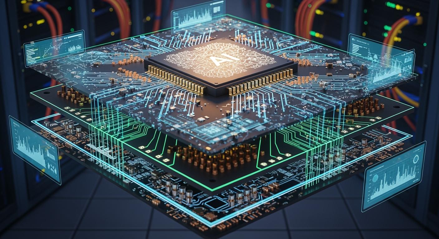
An ideal multi-layer pcb stackup for ai server motherboards uses special layering. This helps high-frequency operations and gives steady power. A multi-layer pcb stack-up means how signal, power, and ground layers are arranged in a pcb. In ai platforms, stack-up complexity affects signal quality, electromagnetic interference, and heat control. For example, a stack-up with 16 to 32 layers allows advanced features and supports many GPU accelerators. Lower layer counts can limit server performance. Engineers must think about pcb stack-up, pcb design, and stackup plans to meet the needs of ai hardware.
Key Takeaways
Multi-layer PCB stack-up lets AI servers work quickly and smoothly.
Adding more layers in a PCB helps signals and power move better.
Engineers pick special materials to keep signals clean and powerful.
A good stack-up design lowers electromagnetic interference.
Putting layers in the right order helps control heat in AI servers.
Ground planes in PCBs help stop noise and make signals better.
Testing checks if the PCB stack-up works well and stays strong.
Multi-layer PCB Stack-up Basics
What Is Multi-layer PCB Stack-up
A multi-layer pcb stackup is how layers are put together in a printed circuit board. Engineers use these layers to move signals, give power, and make ground connections. A multi-layer pcb has three or more layers that carry signals. These layers are placed between sheets of special material called dielectric. This makes the board more complex and gives more ways to connect things. Designers pick a multi-layer pcb stack-up to add advanced features to ai server motherboards.
Multi-layer stackups help boards work better and have less noise in fast systems. They let designers make more complex paths than single or double-layer boards.
Making a multi-layer pcb stackup uses a few important parts. The table below lists the main parts and what they do:
Component | Description |
|---|---|
Layers that carry signals, send power, and make ground connections. | |
Core | Hard material (often FR-4) with copper foil, making the inside layers strong. |
Prepreg | Fiberglass cloth with sticky resin that holds core layers together. |
Designers use these parts to make a stackup that works for ai hardware. The stack-up helps data move fast and keeps power steady. It also cuts down on electromagnetic interference and helps with heat.
Why Stack-up Matters for AI Servers
Stack-up design is very important for ai server motherboards. Engineers need to make a pcb stack-up that can handle fast data and give power well. Ai servers use special hardware like GPUs and TPUs, which need good pcb design. The stack-up must deal with lots of power and heat. Fast channels and special materials in the stack-up keep signals clear and lower signal loss.
A good pcb stack-up makes ai work better. It helps the server run well and do hard jobs. Designers look at how layers are set up, what materials to use, and how layers are spread out. These choices change how good the signals are, how steady the power is, and how heat is handled. A multi-layer pcb stackup lets engineers move signals and power where they need. It also lowers noise and helps with fast work.
Tip: Engineers should check pcb stackup design often to keep up with new ai needs.
Making the stack-up better helps ai server motherboards work their best. It also makes them last longer and easier to build. Designers need to balance signal, power, and ground layers in the stack-up. They pick materials that work well for fast jobs and keep losses low. A strong pcb stack-up design helps ai work and keeps it steady for a long time.
Unique Demands of AI Server PCB Stack-up
AI hardware makes designing multi-layer pcb stackups harder. These systems need very fast speeds and many layers, sometimes 16 to 32. Engineers have to handle lots of data, sudden strong currents, and high heat. Each thing changes how they design the pcb stack-up for powerful computers.
High-Speed Signal Integrity
Signal integrity is a big worry in dense pcbs for AI. Fast signals move through hundreds of lanes, often faster than 28 Gbps. These signals need very tiny timing errors. Engineers face many problems:
Signal integrity problems can come from rough surfaces and the stack-up’s materials.
The layers must stick together well, even as the stack-up gets more complex.
Keeping the right thickness, shape, and flatness is important for good signals.
Fast traces act like transmission lines, so their shape and the stack-up’s materials change how they work.
A good multi-layer pcb stackup keeps signal paths short and straight. This lowers noise and crosstalk, which helps signal integrity in crowded pcbs. Engineers also think about how flat and even the board is, especially with special finishes.
Power Delivery and EMI
Power delivery and EMI are big problems in pcb stack-up design for AI servers. These systems have sudden strong currents when AI chips switch lots of logic at once. The power network must keep voltage steady for the chips to work well.
Some important things to think about are:
High-density connections need thicker copper for power planes to carry strong currents without getting too hot.
Signal layers should stay thin to keep signals clear.
Changing power or signal layers can change EMI, so planning the stack-up is very important.
Even small mistakes in making the layers can break connections, so making the board right is key.
Engineers use special layering in the multi-layer pcb stackup to keep power and signal layers apart. This helps control EMI and keeps power steady for strong computers.
Thermal Management in Multilayer PCB
Thermal management is a key part of multilayer pcb stack-up for AI. Temperatures can go over 120 °C if heat is not removed fast. Engineers use some advanced tricks:
Liquid metal TIMs lower heat resistance much more than old materials.
Self-pressurizing TIMs get bigger with heat, push harder, and move heat better.
Multi-layer TIM stacks, like IBM’s, fix bending in complex stack-ups and keep GPUs cool.
Good thermal management in the pcb stack-up keeps parts safe and makes them last longer. Engineers pick materials and design the stack-up to move heat away from hot spots fast.
Note: The best multi-layer pcb stackup balances signal, power, and heat needs. This balance helps AI and strong computers do tough jobs.
Key Design Considerations for Multi-layer PCB
Layer Count and Arrangement
Engineers pick how many layers a multi-layer pcb stackup needs by looking at how complex the ai hardware is and how many wires must fit. The number of layers changes how the stack-up is made, how signals move, and how power stays steady. Entry-level servers use 10 to 16 layers. These are enough for basic fast signals and okay power sharing. Mid-range ai systems need 16 to 24 layers. This helps balance fast wiring and heat control. High-performance computers use 24 to 40 layers. These boards have lots of wires, thick copper, and their own power sections. Supercomputers and new ai boards can use 40 to 60 layers. These have very tight wiring and tricky stack-ups for fast jobs.
Layer Count Range | Application | Features |
|---|---|---|
10–16 Layers | Entry-level servers, storage controllers, lightweight cloud servers | Basic high-speed signal support, moderate power distribution |
16–24 Layers | Mid-range enterprise servers, dual-CPU platforms, AI inference servers | Balanced high-speed wiring, multiple power planes, good thermal performance |
24–40 Layers | High-performance computing, AI training servers, GPU backplanes, 800G switches | Dense high-speed wiring, independent power domains, thick copper layers |
40–60 Layers | Supercomputers, next-generation AI core boards, Chiplet-based systems | Ultra-high density, Any-layer HDI, complex lamination structures |
The stack-up must fit the ai system’s wiring and signal needs. More layers let engineers split up signal, power, and ground planes. This makes signals better and lowers EMI. Designers use many layers to add new features and keep dense pcbs working well.
Signal, Power, and Ground Layer Distribution
Putting signal, power, and ground layers in the right spots is very important for pcb stack-up. Engineers follow some rules to make the stack-up and signals better in crowded pcbs:
Put fast signals close to ground planes. This cuts down on loop inductance and gives a good path back.
Keep fast and slow signals apart so they do not mix.
Use stripline or microstrip for signal paths. Microstrip works best on the outside, stripline is good inside for shielding.
Put ground planes next to signal layers. This lowers noise and keeps impedance steady.
Use more than one ground plane. This lets each part of the circuit have its own ground and stops noise from spreading.
Do not split ground planes unless you have to. Splitting breaks the return path and makes EMI worse.
Give some layers to certain voltages for steady power.
Put power planes near ground planes. This makes natural capacitance, which lowers noise and keeps voltage steady.
Put decoupling capacitors close to IC power pins. This stops voltage from jumping up and down.
Stack-up design that uses these tips makes signals, power, and EMI better. Engineers get a strong pcb stack-up by planning layers and signal paths well.
Material Selection for Stack-up
Picking the right materials for a multi-layer pcb stackup is very important for ai server speed. The material changes how the stack-up works for fast jobs, signal quality, and how many wires fit.
Low-loss Materials (e.g., Megtron 6/7)
Engineers often use low-loss materials like Megtron 6 or Megtron 7 in ai pcbs. These materials help fast signals and cut down on signal loss. FR4 is cheap and works for most boards, but advanced ai needs materials with lower dielectric constant and dissipation factor.
Material | Key Properties | Applications |
|---|---|---|
FR4 | Cost-effective, good electrical properties, dielectric constant (4.3-4.8), loss tangent (0.015-0.02) | General use in PCBs |
Rogers | Low dielectric constant (2.2-3), low dissipation factor (0.001-0.003) | High-frequency applications (military, communication, space) |
Low-loss materials make signals better in crowded pcbs and help stack-up design for fast computers.
Dk and Df Requirements
Dielectric constant (Dk) and dissipation factor (Df) are important for stack-up design. Engineers pick materials with Dk around 3.5 to 3.7 and Df around 0.010 to 0.012 for PCIe 5.0 or 6.0 stack-ups. Lower Dk means signals get less messed up at high speeds. Lower Df means less energy is lost as signals move.
Property | Typical Value |
|---|---|
Dielectric Constant (Dk) @ 10 GHz | ~3.5–3.7 |
Dissipation Factor (Df) @ 10 GHz | ~0.010–0.012 |
Parameter | Description | Importance |
|---|---|---|
Dk | Dielectric constant | Controls how fast signals move and impedance. Lower Dk means less signal mess-up at high speeds. |
Df | Dissipation factor | Controls how much energy is lost as signals move. Lower Df means less energy lost. |
Stack-up for fast jobs needs materials with the best Dk and Df to keep signals good and losses low.
Signal and Power Integrity
Keeping signals and power steady is very important in pcb stack-up for ai. Engineers use different ways to make multi-layer pcb stack-up work for fast signals.
Decoupling Networks and Copper Pours
Decoupling networks and copper pours help keep voltage steady and lower noise in multi-layer pcb stackup. Engineers put decoupling capacitors close to IC power pins. Copper pours make big ground planes, split up noise, and block antennas. These tricks make power and signals better in crowded pcbs.
Impedance Control and Differential Pairs
Impedance control in multi-layer boards is needed for good signals. Engineers aim for 50Ω single-ended or 100Ω differential impedance using microstrip or stripline. The right stack-up, with signal layers and reference planes, gets the impedance they want. Impedance control stops signals from bouncing back, mixing, or getting lost. Differential pairs help fast signals and make routing better in multi-layer stackup.
Strategy | Description |
|---|---|
Impedance Control | Target 50Ω single-ended or 100Ω differential using microstrip or stripline configurations. |
Ground Plane Optimization | Use continuous ground pours to partition noise domains and stitch splits with vias to block antennas. |
Crosstalk Reduction Techniques | Space parallel traces greater than 3h and route orthogonally across layers to reduce coupling. |
Note: Engineers must make stack-up design better to keep signals, power, and EMI under control in ai server pcb stack-up.
Advanced HDI Strategies
Microvias and Sequential Lamination
Advanced HDI strategies are very important in new stack-up design for AI hardware. These strategies help engineers fit more wires and keep signals strong. They also help deliver power well. High-density pcb designs use microvias and sequential lamination to make multi-layer stackup work better and last longer.
Microvias are tiny holes made by lasers. They connect the outside layers to the inside layers in a multi-layer pcb. This saves space and keeps signal paths short. Shorter paths help signals stay clear in crowded pcbs. This is very important for fast signals. Microvias also lower extra capacitance and inductance. These changes cut down on signal loss and help control impedance in multi-layer boards.
Sequential lamination means engineers build the pcb stack-up step by step. They add layers and microvias in stages. This way, they can make more complex stackups and add more layers without problems. Sequential lamination helps with signal routing. It lets engineers put fast signals on the best layers. It also makes it easier to keep power and ground layers apart. This helps power delivery and controls EMI.
Engineers follow steps to make a strong HDI stack-up for AI systems:
Set design needs, like signal speed, power, and heat limits.
Pick a stack-up type, such as 2+N+2, to balance cost and how well it works.
Plan signal paths to keep pairs together and control impedance in multi-layer boards.
Use thick copper layers for good power and heat control.
Add thermal vias to move heat away from hot spots.
Choose the right via types, like microvias, to save space and make the board stronger.
Check trace width and space before making the board.
Work with skilled fabricators who know HDI stackup design.
Microvias and sequential lamination let engineers fit more wires and parts in a small space. For example, smartphone motherboards use microvias to fit more parts and keep signals clear at high speeds. In AI server pcb stack-up, these tricks let engineers route many fast signals across layers without losing signal quality.
The table below shows how microvias and sequential lamination help stack-up design:
Feature | Benefit for Stack-up Design |
|---|---|
Microvias | Shorter signal paths, better signal integrity, higher routing density |
Sequential Lamination | More layers, flexible stackup, improved reliability |
Thermal Vias | Better heat management, safer components |
Thick Copper Layers | Stronger power delivery, less voltage drop |
Tip: Engineers should always check stackup design and routing plans with fabricators. This makes sure the multi-layer pcb works well and lasts a long time.
Advanced HDI strategies, like microvias and sequential lamination, help engineers build tricky pcb stack-up structures for AI hardware. These methods make signal routing better, fit more wires, and support the fast signals needed in new AI systems.
Best Practices and Pitfalls in PCB Stack-up
Optimizing Multi-layer PCB Stackup
Engineers plan how many layers to use early. They decide where each layer goes before making the pcb. Using symmetry in the stack-up helps stop the board from bending. Teams talk to manufacturers from the start to make sure the stack-up can be built. They use tests and computer models to check signals and heat before finishing the design. Keeping the right impedance is very important for fast signals.
A good stack-up has special layers for signal, power, and ground. Designers put fast signal layers next to ground planes to lower noise. This makes signals clearer. They keep wires short and straight to stop signal loss. Power planes are close to ground layers. This helps with natural capacitance and keeps voltage steady. Decoupling capacitors near ICs help give steady power.
Tip: Engineers should always use simulation tools to check for signal problems early.
Working with fabricators helps make sure the stack-up can be made. Teams pick materials that fit the speed and density needed for ai hardware. They check if the stack-up can move heat away from hot spots. Using microvias and sequential lamination lets them add more layers and better routing in tight spaces.
The table below lists key steps for making a good stack-up:
Step | Benefit |
|---|---|
Early planning | Fewer design changes |
Symmetrical layers | Less board warping |
Simulation/testing | Better signal integrity |
Reliable high-speed signals | |
Manufacturer input | Feasible pcb stack-up |
Common Mistakes in Stack-up Design
Many teams make mistakes in pcb stack-up that hurt ai server performance. One mistake is not keeping fast signal layers away from noisy power layers. This can cause signal loss and more EMI. Some designers split ground planes, which breaks the return path and adds noise. Using uneven layers can make the board bend or warp.
If teams ignore impedance control, signals can bounce back and get weak. Sometimes teams forget to test the stack-up, so they miss routing or heat problems. Picking the wrong materials can slow down the board and lose signals. Putting too many wires on one layer makes routing hard and causes crosstalk.
Note: Do not split ground planes and always check the stack-up for good signal and power paths.
Engineers should always work with manufacturers to avoid problems when making the board. They must check if the stack-up can be built and will last. Teams should not put decoupling capacitors far from ICs, or power delivery will be weak. They need to check for thermal vias and thick copper layers to handle heat.
A strong pcb stack-up avoids these mistakes and helps ai servers work well. Teams who follow best practices get clear signals, steady power, and reliable boards.
Example Multilayer PCB Stack-up Configurations
16-layer PCB Stack-up Example
A 16-layer stack-up is a strong choice for mid-range AI servers. This stack-up lets engineers use fast wiring and many power planes. Designers pick this setup for AI inference servers and enterprise platforms. The stack-up usually has:
Four to six signal layers for fast data paths.
Several ground layers to help signals stay clear.
Multiple power layers for steady voltage.
Careful layer order to lower EMI.
A normal 16-layer pcb stack-up might look like this:
Layer | Function |
|---|---|
1 | Signal |
2 | Ground |
3 | Signal |
4 | Power |
5 | Signal |
6 | Ground |
7 | Signal |
8 | Power |
9 | Power |
10 | Signal |
11 | Ground |
12 | Signal |
13 | Power |
14 | Signal |
15 | Ground |
16 | Signal |
This stack-up keeps signal paths short and neat. Engineers can handle lots of wires and keep signals strong.
24-layer PCB Stack-up Example
A 24-layer stack-up is used for high-performance AI training servers. This setup lets engineers use dense wiring and separate power domains. Thick copper layers help with power and heat. The stack-up often has:
Eight or more signal layers for tricky routing.
Several ground layers for strong EMI shielding.
Power layers for each voltage domain.
Extra layers for heat control.
A 24-layer pcb stack-up lets engineers route many signals without crosstalk. It also supports advanced features like DDR5 and PCIe Gen 5. The table below compares the two stack-ups:
Layer Count | Application | Features |
|---|---|---|
16 Layers | Mid-range enterprise servers, AI inference servers | Balanced fast wiring, many power planes, good heat control |
24 Layers | High-performance computing, AI training servers | Dense wiring, separate power domains, thick copper layers |
Note: A 24-layer stack-up gives more routing choices and better signal strength for tough AI jobs.
Comparing Stack-up Approaches
Different stack-up setups have their own good and bad points. Engineers pick a stack-up based on what the AI server needs. For example, a 16-layer pcb stack-up balances cost and performance. It works well for most enterprise jobs. A 24-layer pcb stack-up supports more wires and better signal control. This is important for AI training and fast data.
The table below shows how stack-up choices change design:
Layer Configuration | Advantages | Disadvantages | Applicable Scenarios |
|---|---|---|---|
16-layer stack-up | Good signal strength, balanced power, lower cost | Less space for tricky designs | Mid-range AI servers, inference platforms |
24-layer stack-up | Better signal strength, high wiring density | Higher cost, harder to make | AI training servers, HPC, dense platforms |
Engineers must match the stack-up to the server’s needs. More layers give better signals and routing, but cost more and are harder to build. Careful stack-up planning makes sure every AI server works well.
Manufacturing and Validation for PCB Stack-up
Fabrication Challenges
Making a multi-layer stack-up for AI servers is hard. Engineers must plan each step to keep the stack-up strong. The materials and how layers work together are very important. Mechanical and electrical parts must fit well for fast signals.
Some main challenges in stack-up fabrication are:
Planning materials and via types for dense routing and strong signals.
Managing lamination with heat and pressure to bond layers. Each cycle must keep the stack-up flat and lined up.
Making sure all layers line up perfectly. Even a small shift can break signals or cause shorts.
Using sequential lamination and microvias to add more layers. This keeps signal quality high.
Controlling plating thickness in vias to stop failures from heat.
Following best practices for impedance planning to keep signals strong.
Meeting industry standards and test methods for every stack-up.
Manufacturing tolerances change how reliable each stack-up is. If layers do not line up, vias and traces can miss their targets. This can break signals or cause shorts. Bad plating or heat stress can make vias fail. This hurts both signals and power. Not enough space or grounding can cause crosstalk and EMI. This lowers performance in fast AI servers.
Testing and Reliability
Testing and validation make sure each stack-up meets quality standards. Engineers use many ways to check the stack-up after making the pcb. Time Domain Reflectometry (TDR) checks impedance along signal paths. Vector Network Analyzers (VNA) check RF performance for fast signals. Automated Optical Inspection (AOI) finds defects in layers, traces, and vias. These tests help find problems early and keep the stack-up reliable.
Quality control helps every step of pcb manufacturing. International standards like ISO9001 and IPC-A-610H guide the work. These standards make sure stack-up production is consistent and traceable. AOI and X-ray inspections check for hidden faults in layers and vias. UL and RoHS certifications confirm safety and environmental rules. Production records track every stack-up for full traceability.
A skilled engineering team can make the stack-up structure better to lower costs. They keep signal integrity and EMC performance high. They work with fabricators to pick the right materials, plan routing, and manage layers for each 22 layer pcb. This teamwork makes sure every stack-up supports fast signals and dense routing in AI servers.
Note: Reliable stack-up design, careful pcb manufacturing, and strong testing keep AI servers running at top performance.
Stack-up design is important for how well AI servers work. Engineers pick layers that help signals move fast and keep power steady. They plan the stack-up to lower EMI and make routing easier. Teams pick materials that keep signals strong and stop signal loss. Using a symmetrical stack-up stops the board from bending during pcb manufacturing. Continuous reference planes help signals stay clear and strong. The table below shows how stack-up choices affect server reliability and how easy it is to make:
Aspect | Description |
|---|---|
Signal Integrity | Stack-up design sets limits for fast signals. |
Power Integrity | Layer order keeps power steady and helps performance. |
EMC | Good stack-up planning lowers EMI for better server work. |
Material Selection | Special low-loss materials help signals at high speeds. |
Layer Sequencing | Symmetrical stack-up stops boards from bending or twisting. |
Reference Plane Continuity | Continuous planes stop signal bounce and keep signals strong. |
Teams should check stack-up plans, talk to experts, and use best practices. Careful stack-up design gives strong signals, good layers, and easy routing in every 22 layer pcb.
FAQ
What is the main benefit of a multi-layer PCB stack-up in AI servers?
A multi-layer PCB stack-up lets engineers send fast signals and give steady power. This design helps advanced AI hardware work well and lowers electromagnetic interference.
How many layers do most AI server PCBs use?
Most AI server PCBs have 16 to 32 layers. High-performance systems can use even more layers for tight wiring and special features.
Why do engineers choose low-loss materials for AI server PCBs?
Low-loss materials like Megtron 6 or 7 help signals move faster and cut down on signal loss. These materials make high-speed AI server jobs work better.
How does stack-up design affect thermal management?
Stack-up design helps heat move away from hot parts. Engineers use special materials, thick copper, and thermal vias to keep things cool and make parts last longer.
What is the role of ground planes in PCB stack-up?
Ground planes give signals a way back and help control noise. They also lower electromagnetic interference and make signals stronger.
Can improper stack-up design cause server failures?
Yes. Bad stack-up design can cause signal loss, power trouble, or too much heat. These problems can make servers unstable or break hardware.
How do engineers test the reliability of a PCB stack-up?
Engineers use tools like TDR, AOI, and X-ray checks. These tests look for problems, measure impedance, and make sure the stack-up is good.
See Also
Understanding Common Stack-up Configurations for HDI PCBs
Diverse Uses of Multilayer PCBs in Various Sectors
Evaluating Costs and Benefits of Advanced HDI PCB Designs
Guide to Manufacturing Techniques for Heavy Copper PCBs
Challenges in Manufacturing and Prototyping Multilayer Circuit Boards