Multi-layer PCB Lamination Design Mistakes & Solutions
You can make important mistakes in PCB Lamination Design. These mistakes can hurt the board’s quality and how well it works.
Delamination, voids, warpage, and registration problems can make signals weak or stop working in tough jobs.
If you do not balance stackups, pick the right via, use enough copper, or follow manufacturing rules, you can get problems with the board’s structure and electricity.
If you find defects like voids or wrong lamination pressure early, you can stop signal problems and keep the board working for a long time. You will learn useful ways to make your board work better and last longer.
Key Takeaways
Keep materials dry and clean to stop delamination and voids. This keeps connections strong and signals clear.
Use the right spacing rules to stop crosstalk and electrical problems. Good spacing keeps signals strong and lowers costs.
Pick the best materials for your PCB to handle heat and stress. Good materials stop overheating and signal loss.
Watch the lamination process closely. Use even pressure and heat to stop problems like warping and misalignment.
Check your boards after lamination. Finding problems early helps make boards work well and last longer.
Common Multi-layer PCB Lamination Mistakes
Delamination and Voids
Delamination and voids can happen in multi-layer PCB lamination. Delamination is when layers come apart or lose their stickiness. Voids are air bubbles or spaces between layers. These mistakes make the board weaker and mess up signals.
Delamination starts when water gets stuck in prepreg or core materials. When you heat these materials over 180°C, water turns into steam and breaks the bond. If you use resins that soak up more than 0.5% water, delamination happens more often.
Dust, oil, or leftover stuff on copper or fiberglass stops resin from sticking. Wrong lamination settings, like too much or too little pressure, can trap air or make tiny cracks. Layers can also come apart if they cool too fast and do not match well. Voids show up when air gets trapped or resin does not spread right. These spaces make the board weaker and mess up signals, especially in high-frequency designs.
Moisture absorption
Contamination
Incorrect lamination parameters
Thermal mismatch
Voids from trapped air or poor resin flow
Warpage and Wrinkling
Warpage and wrinkling make the PCB bend or wrinkle. You see these mistakes when prepregs have uneven resin or are cut badly. Bent core boards do not stay flat and cause stress wrinkles.
Bad lamination settings, like fast temperature changes or uneven pressure, make wrinkles. Stacking carelessly and trapping air bubbles also cause misalignment and wrinkling.
Uneven resin content in prepregs
Warped core boards
Rapid temperature changes
Uneven pressure
Misaligned stacking
Wrinkles cause drilling mistakes and batch rejections.
They change impedance and move pads out of place.
Hidden wrinkles can break during heating and cooling, causing sudden failures.
Layer Misalignment
Layer misalignment happens when layers move during lamination. You see traces and pads in the wrong spots. This mistake makes crosstalk and signal loss worse, especially in high-frequency designs.
Misalignment causes impedance mismatch and system failures. Resin flow, layer registration, pressure balance, heating, cooling, and material expansion all affect alignment.
Layer shift during lamination
Misaligned traces and pads
Crosstalk and signal loss
Impedance mismatch
System failures
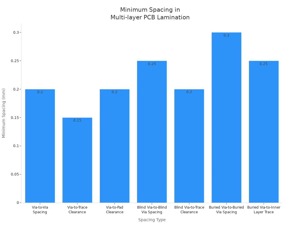
Inadequate Spacing and Crowding
Inadequate spacing and crowding cause problems in multi-layer PCB lamination. You must follow rules for spacing between vias, traces, and pads. If you ignore these rules, you get drilling mistakes, short circuits, and weak connections.
Close spacing causes crosstalk and electrical interference, especially in fast designs. Bad spacing also makes heat build up and raises manufacturing costs.
Spacing Type | Minimum Spacing | Reason/Impact |
|---|---|---|
Via-to-Via Spacing | 0.2 mm (8 mils) | Stops drilling mistakes and keeps the board strong. |
Via-to-Trace Clearance | 0.15 mm (6 mils) | Stops short circuits and electrical interference. |
Via-to-Pad Clearance | 0.2 mm (8 mils) | Stops solder from bridging during assembly. |
Blind Via-to-Blind Via Spacing | 0.25 mm (10 mils) | Stops overlap during laser drilling and keeps vias strong. |
Blind Via-to-Trace Clearance | 0.2 mm (8 mils) | Lowers electrical interference in fast designs. |
Buried Via-to-Buried Via Spacing | 0.3 mm (12 mils) | Helps with alignment during lamination and drilling inside layers. |
Buried Via-to-Inner Layer Trace | 0.25 mm (10 mils) | Stops signal crosstalk and keeps impedance control. |
Manufacturing gets less accurate with bad spacing.
Signal quality drops with close vias.
Heat builds up with crowded parts.
Costs go up with tight spacing.
Material Selection Errors
Material selection errors change how the board handles heat and stress. If you pick the wrong materials, you get signal loss, overheating, and warping.
The materials you choose decide how well your board deals with heat, stress, and making. Bad choices cause reliability problems and cost more.
You must pick materials that fit your design. Bad choices can cause hidden problems and make the board work worse.
Layer Count Inflation
Layer count inflation means you add more layers than needed. This mistake costs more and makes manufacturing harder.
If you do not plan your stack-up well, you lose yield and reliability. Thin PCBs may seem cheaper, but they bend and crack easily.
Bad stack-up planning and extra layers cause more failures and higher costs.
Poor stack-up planning
Unnecessary layer count
Higher costs
Reduced yield
Reliability problems
You must avoid these mistakes to make your multi-layer PCB better and more reliable.
Effects on Multilayer PCB Performance
Electrical Failures
Lamination defects can cause big electrical failures in your PCB. Delamination makes layers come apart and weakens the board. Voids trap air between prepreg and copper, especially near vias or thick copper spots. These problems can:
Stop signals from moving because of open circuits.
Change impedance and make signals not work right.
Lower insulation resistance and let bad currents leak.
Cause thermal failure when heat hurts the board.
Make via reliability worse and break connections.
Lead to assembly defects that make the board hard to use.
If you make boards for cars, factories, or medical tools, delamination can make the whole product fail. Voids let moisture in, which breaks insulation and spreads cracks when the board heats up or cools down.
Mechanical Reliability Issues
Mechanical reliability gets worse with lamination mistakes. You see weaker copper-to-resin bonds and more micro-cracks after heating and cooling. Peel strength drops, and the board can grow conductive anodic filaments (CAF). Bad defects can split layers and cause early failures.
Blisters show up on the board’s surface.
Discoloration appears in some spots.
Intermittent opens happen during electrical tests.
You need to look for these signs. They warn you about hidden problems that can make your product not last long.
Manufacturing Yield Losses
Lamination defects lower how many good boards you make. You waste boards with delamination, voids, or misalignment. You spend more time and money fixing these problems. Yield losses mean fewer boards pass checks and more get thrown away.
Defect Type | Impact on Yield | Common Result |
|---|---|---|
Delamination | High scrap rate | Product failure |
Voids | Increased rework | Reliability issues |
Misalignment | Batch rejection | Cost escalation |
🛠️ Careful design and process control help you stop these losses. You make boards more reliable and save money when you prevent lamination mistakes.
Prevent PCB Lamination Issues: Solutions & Best Practices
Material and Prepreg Selection
Pick the right materials and prepregs for your board. Matching material properties stops stress and warping. Using FR-4 with a similar thermal expansion keeps layers together. Store prepreg and core materials in a dry place. Keep humidity under 50%. Bake them at 120°C for a few hours before lamination. This step removes moisture and stops delamination.
Clean copper surfaces before you start. Roughen them to 1-2 μm. This step helps layers stick together. Pick prepreg with resin content between 40-50% for FR-4. This choice makes resin flow well and fills gaps. Heat and cool slowly, about 2-3°C per minute. This step lowers thermal stress. Keep vacuum pressure at least 25 inHg during lamination. This pressure removes air and stops voids.
Tip: Always check the lamination temperature for your material. For FR-4, keep it between 180-200°C. This range helps resin flow and stops breakdown.
Optimized Layer Stack-up
Balance your layer stack-up to stop lamination issues. Symmetry keeps stress even and stops warping. Match core and prepreg thickness across cycles. This step keeps dielectric constants steady and helps with impedance control.
Key Aspect | Explanation |
|---|---|
Symmetry | Balanced layers lower warpage during lamination. |
Core and Prepreg Thickness | Matching thickness keeps dielectric constants steady. |
Material Selection | Low thermal expansion materials stop stress buildup. |
Arrange vias to lower lamination cycles. Fewer cycles mean less stress. Plan your stack-up for material shrinkage. This step keeps sizes accurate.
Note: Mirror copper patterns on top and bottom layers of a 4-layer board. This step balances copper and stops uneven stress.
Process Control and Pressing Techniques
Control the lamination process to stop defects. Advanced presses use controllers to keep pressure even. Match temperature and pressure to stop thermal stress and cure evenly.
Use cushioning materials to spread pressure. This step lowers overpressure risk. Sensors track pressure in real time. Automatic changes stop defects like delamination, voids, and warping.
Optimize heating for good resin flow and curing.
Add vacuum degassing to remove leftover gases.
Keep humidity under 40% RH to stop lamination issues.
🛠️ Using these controls helps you avoid delamination, air bubbles, and warping.
Spacing and Layout Guidelines
Follow spacing and layout rules to build strong boards. Give enough space for assembly. This step stops parts from hitting each other. Keep component orientation the same to make assembly easier. Leave space around edges to stop crowding.
Group similar parts to make layout better. Do not put power parts together. This step stops overheating and hot spots. Space out heat-making parts to help heat move away. Put parts where air can flow.
Do not cluster power parts.
Place parts for good heat management.
Give enough space for assembly.
Tip: Good spacing makes signals better and lowers costs.
Managing Layer Count
Manage layer count to lower complexity and stop lamination issues. More layers make more heat and harder cooling. Sequential lamination keeps alignment and bonding strong. This step lowers defects in multi-layer boards.
Evidence Type | Description |
|---|---|
Thermal Management | More layers make more heat and harder cooling. |
Structural Integrity | Sequential lamination keeps alignment and bonding strong. |
Complexity and Cost | More layers make things harder and risk more defects. Fewer layers are often enough. |
Note: Plan your stack-up carefully. Use only the layers you need. This step lowers costs and makes boards more reliable.
Cleanliness and Surface Preparation
Cleanliness and surface prep are important in lamination. Keep rooms clean and control humidity. Dust-free rooms lower contamination and help layers stick. Clean copper with chemicals or plasma. This step makes bonding better and lines more accurate.
Evidence Type | Description |
|---|---|
Strict Environmental Control | Clean rooms with low humidity and no dust lower contamination. |
Insufficient Cleanliness Before Lamination | Dust, oils, or residue stop bonding and cause defects like delamination. |
Enhanced Surface Preparation | Cleaning copper well helps layers stick and lines form right. |
🧼 Always check for dust, oil, or residue before lamination. Clean surfaces help you avoid problems and build strong boards.
You can stop lamination issues by following these best practices. If you pick the right materials, balance your stack-up, control the process, follow spacing rules, manage layer count, and keep surfaces clean, you will build strong multi-layer boards with fewer problems.
Inspection and Testing in PCB Lamination Design
Post-lamination Quality Checks
You need to check your PCB after lamination. These checks help you find problems early. If you check now, you can fix mistakes before shipping. You can look at the board to find delamination, warpage, or wrinkling. You can also check if the board is flat and look for air bubbles. AOI machines scan the board’s surface for problems. X-ray inspection lets you see inside the board. It helps you find hidden voids or layers that do not line up.
Microsectioning lets you look closely at copper and dielectric layers. This helps you find cracks or delamination. Continuity and isolation tests check if the board’s circuits work. These tests show if there are open circuits or shorts.
Test type | Parameter | Typical value | IPC limit |
|---|---|---|---|
Continuity | Test voltage | 10 V | Application-based |
Continuity | Measurement current | 30 mA | Application-based |
Continuity | Max resistance (pass) | 10 Ω | Up to 100 Ω |
Isolation | Min resistance (pass) | ≥ 20 MΩ | Standard IPC |
You should also test how the board handles heat. These tests show if problems happen when the board gets hot. Thermal cycling checks if layers stay together when the temperature changes.
Detecting and Addressing Defects
You need special tools to find and fix defects. X-ray inspection helps you see inside the board for voids or delamination. Boundary scan testing checks if crowded board connections work. Capacitive testing finds problems in small parts. 4-wire Kelvin testing checks resistance in important spots.
Looking at the board helps you find surface problems.
Checking process data shows if settings caused mistakes.
Material testing finds problems from water or bad resin.
Real-time monitors catch problems as soon as they happen.
Rules make you use safer materials and better ways to build boards. These rules help stop problems and make boards last longer. You must follow limits on dangerous stuff and VOCs. Closed-loop cleaning keeps boards clean and stops contamination.
If you only check a few boards, you might miss some problems. Real-time feedback helps you fix mistakes right away. Keep vacuum low and control resin to stop air bubbles and voids. Clean rooms and slow temperature changes help avoid problems during lamination.
If you find and fix problems early, your boards will last longer and work better.
You can stop most multilayer problems by doing a few things.
Design your board so it is easy to make. This lowers mistakes and saves money.
Try to use fewer layers in high-frequency and high-speed designs.
Pick common materials for multi-layer printed circuit boards. Make sure your board size is good.
Control your process and use AOI, X-ray, and AI inspection. These tools help you find problems early.
Clean the board’s surfaces and check for special issues in registered multi-layer boards.
If you plan ahead and keep improving, your signals will work better and your board will last longer. New inspection tools help you spot problems before they break your board. Always care about quality and look for ways to make your multilayer process better.
FAQ
What causes delamination in pcb lamination design?
Delamination happens when water gets stuck in the layers. You should keep all materials dry and clean. Delamination makes high-frequency and high-speed signals worse. Always check prepreg and core before you start lamination. Delamination makes high-frequency pcb designs less reliable.
How does spacing affect high-frequency and high-speed pcb lamination design?
You need to follow spacing rules in pcb lamination design. If parts are too close, crosstalk happens in high-frequency and high-speed boards. This can cause signal loss and interference. Good spacing keeps signals strong. Always check spacing for high-frequency and high-speed layouts.
Why is material selection important for high-frequency and high-speed pcb lamination design?
You should pick materials with low loss for high-frequency and high-speed boards. If you use the wrong materials, you get signal loss and overheating. You might see warping and weak signals. Good material choice helps pcb lamination design work well for high-frequency and high-speed uses.
How do you prevent layer misalignment in pcb lamination design for high-frequency and high-speed boards?
You need to use tools that line up layers exactly. You should control temperature and pressure during lamination. Layer misalignment causes signal loss in high-frequency and high-speed designs. You might see impedance mismatch and system failures. Careful pcb lamination design helps stop misalignment.
What tests help you check pcb lamination design for high-frequency and high-speed boards?
You can use AOI, X-ray, and microsectioning to test boards. These tests help you find defects in pcb lamination design. You should check for delamination, voids, and misalignment. Testing keeps high-frequency and high-speed boards working well. Good inspection means fewer failures.
See Also
Challenges In Producing Multi-Layer Circuit Boards And Prototypes
Essential Skills For Designing Multi-Layer PCB Layouts Effectively
Understanding The Comprehensive Process Of Creating Multilayer PCBs
Addressing Common PCB Design Issues For SMT Technology Needs
Exploring Buried Via Technology In Multilayer PCBs And Solutions