PCB AOI Testing helps you avoid costly errors
PCB AOI Testing is a reliable way to prevent expensive mistakes in making PCBs. You use special cameras to check every board for problems. Quality control is important because small mistakes can cause big trouble. AOI helps you find these problems early. This protects your money and keeps your products working well.
Quality control in PCB production helps you save money and makes your customers trust you.
Key Takeaways
PCB AOI Testing uses special cameras to find problems fast. It checks printed circuit boards and saves time. This also helps stop expensive mistakes from happening.
Using AOI at important steps helps spot issues early. This makes the boards better and means less fixing later.
AOI systems can check more than 5,000 boards every hour. They work much faster and are more accurate than people checking by hand.
Checking AOI often and having clear rules for defects helps it work better. This means the boards are checked well and quality stays high.
AOI helps companies save a lot of money. It does this by lowering mistakes and making production smoother.
PCB AOI Testing Overview
What Is AOI?
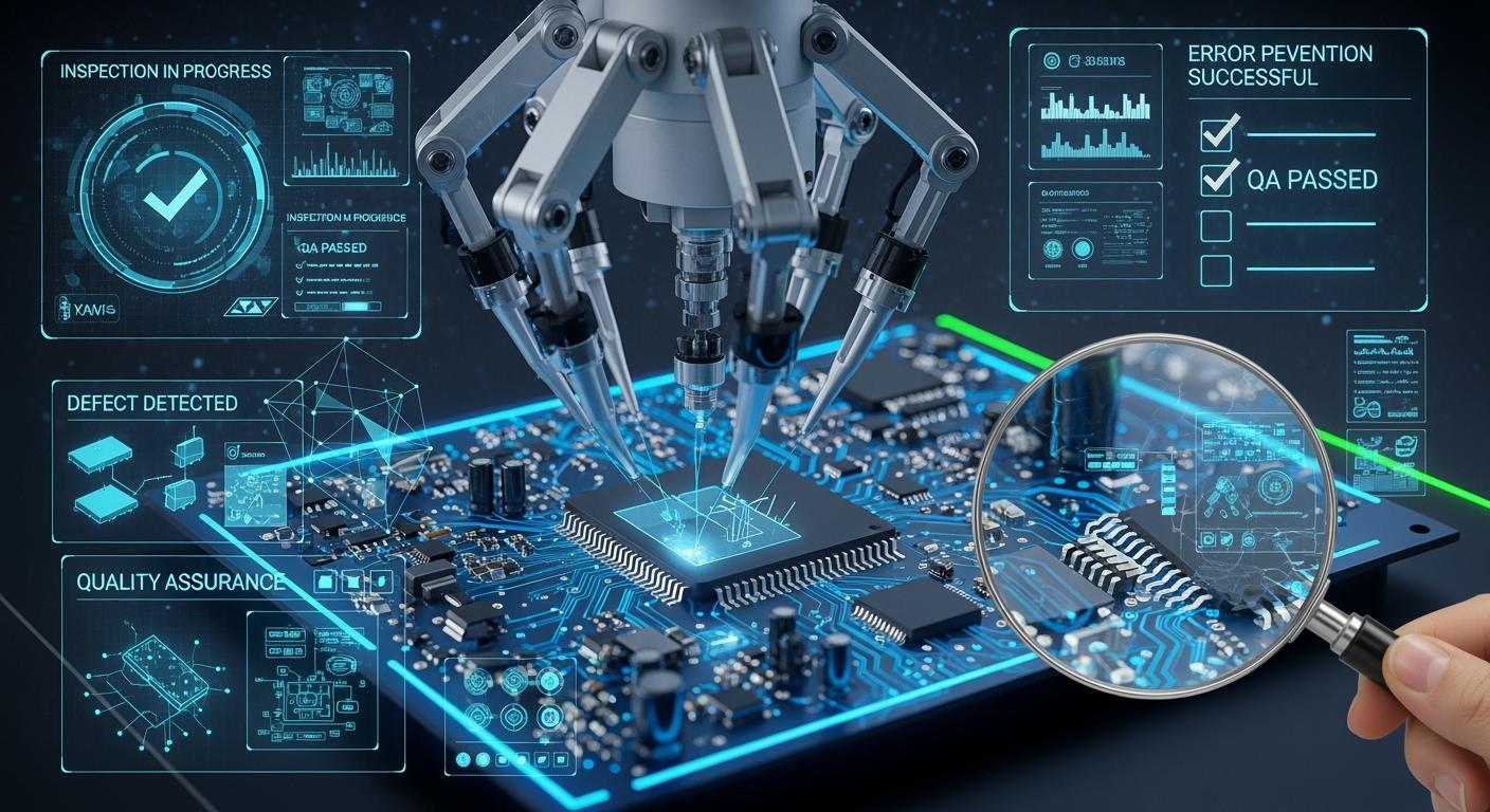
Automated Optical Inspection, or AOI, checks printed circuit boards for problems. AOI uses cameras with high detail and bright lights to take pictures of each board. These pictures help you see if there are scratches, stains, missing pieces, or soldering issues. The system looks at the board and compares it to a perfect board or design plans. Some AOI systems use 3D pictures to measure how tall and shaped the solder joints are. This helps you find pins that are lifted or weak spots.
AOI works quickly and is very accurate. You can check up to 100 boards in one hour. This is much faster than checking by hand. The machine does not touch the board, so it does not cause damage. AOI uses smart computer programs to find even very small mistakes. As electronics get smaller and harder to make, AOI keeps getting better with artificial intelligence and machine learning. This means you can find new kinds of problems as they show up.
AOI helps your factory run well and keeps your boards from having expensive mistakes.
Role in PCB Manufacturing
You can use AOI at different steps when making PCBs. For example, you can use it after putting on solder paste to check its height and shape. You can also use AOI after putting on parts to make sure everything is in the right place and facing the right way. After soldering, AOI looks for problems like tombstoning or solder bridges.
Here’s how AOI fits into your work:
Stage of Integration | Purpose of AOI Inspection | Benefits of Integration |
|---|---|---|
After solder paste printing | Checks paste height, shape, and alignment | Reduces errors early in the process |
After component placement | Verifies presence, orientation, and alignment of parts | Prevents rework and ensures quality |
After reflow soldering | Inspects solder joints for defects | Confirms boards meet quality standards |
PCB AOI Testing is now used in many factories all over the world, especially in electronics and cars. You see AOI in Asia, North America, and Europe. As factories get smarter, AOI connects with AI and IoT to make quality control even better.
Common PCB Errors Detected by AOI
Surface Defects
There are many surface defects you can find on a printed circuit board. These problems can make your board stop working or work badly. PCB AOI Testing helps you find these problems early. Here are some common surface defects you might see:
Scratches: These are marks or lines that can break connections.
Stains: These are spots or dirt that can cause rust.
Damaged traces: These are broken lines that stop electricity.
Excess copper: Extra metal left can make short circuits.
Solder mask misregistration: The cover does not line up and leaves parts open.
AOI systems use special cameras to find these problems. You can see even small scratches or stains that are hard to see with your eyes.
AOI also finds pattern problems, like lines that are too wide or too thin. AOI checks your board by comparing it to a perfect design. If something is wrong, you get a warning.
Dimensional Defects
Dimensional defects happen when the size or shape of parts is wrong. These mistakes can make your board not work. PCB AOI Testing helps you find these problems fast. Here are some examples:
Open traces: Gaps in lines that stop signals.
Short circuits: Lines touch when they should not.
Line width violations: Lines are too thick or too thin.
Spacing violations: Gaps between lines are too small.
Missing or undersized pads: Places for parts are too small or gone.
Unwanted copper: Extra metal left after making the board.
Via defects: Holes are not in the right place or are broken.
AOI uses cameras and smart software to check every part of your board. The system takes pictures and compares them to a perfect board or your design file. If it finds a problem, you get a warning right away. AOI can use both 2D and 3D images to check size and placement. This makes the inspection very good.
You can trust AOI to find almost all dimensional defects. Some checks, like polarity, can be almost perfect.
Missing Components
Missing components are a common problem when making PCBs. If a part is missing, your board will not work right. You might see empty spots where a resistor, capacitor, or chip should be. PCB AOI Testing helps you find these missing parts fast.
Missing resistors
Missing capacitors
Missing chips or integrated circuits
Missing connectors
AOI systems look at your board and compare it to the design file. The cameras take clear pictures and the software checks if every part is there. If a part is missing, you get a warning right away. This helps you fix the problem before the board leaves the factory.
AOI does not just find missing parts. It also checks if parts are in the right place, facing the right way, and have the correct value.
Here is a table that shows how AOI finds different types of errors:
Defect Category | Examples | Impact on Board | AOI Detection Strength |
|---|---|---|---|
Component Issues | Misplacement, rotation, missing parts | Open circuits, short circuits | Excellent (position & presence) |
Solder Defects | Insufficient/excess solder, bridging | Weak joints, shorts | Very strong (especially 3D) |
Polarity Errors | Reversed diodes, capacitors, ICs | Functional failure | High (marking & orientation) |
Surface Anomalies | Scratches, contamination, damaged traces | Reliability issues, corrosion | Strong (visual contrast) |
Tombstoning/Billboarding | Lifted or upright components | Intermittent connections, opens | Excellent (3D height measurement) |
You can see that PCB AOI Testing gives you strong protection from many types of errors. You save time and money by finding problems early.
AOI Detection Process
Camera Technology
You use advanced camera technology in AOI systems to check every part of your PCB. High-speed cameras scan the board from different angles. These cameras use bright lights, such as white, RGB, and angled lighting, to make every detail clear. You can see the edges of components and the shape of solder joints. The system captures images quickly and sends them to a computer for analysis.
Here is how the process works:
Image capture: Cameras scan the PCB using several light sources.
Reference matching: The system compares the images with perfect boards and design files.
Defect detection: Software looks for mistakes like misplaced parts or bad solder joints.
Classification and output: The system sorts the problems and shows them to you for review.
You get fast and accurate results with this method. The cameras do not touch the board, so you avoid damage. You can trust the system to find even tiny errors that are hard to see with your eyes.
2D and 3D Inspection
You can use both 2D and 3D inspection in PCB AOI Testing. In 2D inspection, the system takes flat pictures of the board. This helps you find surface problems, missing parts, and wrong placements. In 3D inspection, the system measures the height and shape of solder joints and components. You can spot lifted pins, tombstoning, and weak solder connections.
AOI systems work much faster than manual inspection. Look at this table to see the difference:
Inspection Method | Components Inspected per Hour |
|---|---|
AOI Systems | Over 5,000 |
Manual Inspection | 500-800 |
You save time and money because AOI checks more boards in less time. You also get better quality because the system does not get tired or miss small details. With 2D and 3D inspection, you make sure your boards meet high standards before they leave the factory.
Tip: Use both 2D and 3D AOI to catch more types of errors and improve your quality control.
AOI vs. Manual Inspection
Accuracy Comparison
You want your PCBs to work well every time. Manual inspection means people look at each board. People can get tired and miss small problems. AOI uses cameras and computers to check every detail. This helps you find more mistakes before boards leave the factory.
AOI systems never get tired or lose focus. You get the same careful check every single time.
See how defect detection rates are different:
Inspection Method | Defect Detection Rate |
|---|---|
AOI | Above 95% |
Manual Inspection | 10-20% error rate |
AOI finds almost all defects on your boards. Manual inspection can miss many problems, especially with small or complex boards. PCB AOI Testing helps you keep quality high and customers happy.
Cost Savings
You also want to save money when making PCBs. AOI helps you do this in a few ways. You spend less time fixing mistakes because you catch them early. You also avoid sending bad boards to customers. This saves you from returns and repairs.
Here is a table that shows how AOI and manual inspection compare for saving money:
Aspect | AOI | Manual Inspection |
|---|---|---|
ROI Timeframe | 14-18 months | N/A |
Defect Rate Reduction | Up to 40% fewer errors | N/A |
Cost Efficiency | Better for high-volume | Better for small batches (under 1,000 boards) |
You get your money back in about a year and a half with AOI. You also see up to 40% fewer mistakes. If you make lots of boards, AOI gives you better value. Manual inspection works for very small batches, but it cannot match AOI for speed or savings.
Tip: Use AOI for big production runs to save money and improve quality.
Benefits and Best Practices
Quality Improvement
When you use PCB AOI Testing, your quality gets much better. This system helps you find problems quickly and very accurately. You can spot soldering flaws, misplaced parts, and surface defects before they get worse. You do not need to redo work as much, and you throw away fewer boards. This saves you both time and money.
Here are some main benefits you get from AOI:
You find defects faster, more accurately, and every time.
You stop soldering flaws, wrong part placement, and surface problems.
You do less rework and scrap, so your factory works better.
You also get these big advantages:
You catch even tiny defects with high accuracy.
You check up to 100 boards each hour, which is fast.
You save money by fixing problems early and avoiding recalls.
Many companies have seen these results. Some saved $1 for each board and did half as much rework. They also saw what was happening in real time and saved thousands every month. Finding problems early means fewer returns and less waste.
Metric | Outcome |
|---|---|
Cost Savings per Unit | $1/unit |
Reduction in Rework | 50% |
Real-time Visibility | Thousands of dollars per month |
Engineering Time Savings | Several thousands per month |
Increased Yield | Fewer returns and less scrap |
AOI lets you see your process clearly and helps your team work together better.
Implementation Tips
You get the best results from AOI if you follow some good steps. Calibrate your system often to keep it working right. Make clear rules for what counts as a defect. Put AOI checks after important steps, like after placing parts and after soldering. Teach your team how to read AOI reports and focus on the most important things.
Here are some tips to help you do well:
Calibrate your AOI system often and update your reference data.
Set clear rules for defects using industry standards.
Put AOI after key steps to catch problems early.
Train your staff to read AOI reports and take action.
Keep a list of defects to help find repeat problems.
You can also:
Connect AOI data to your quality system to see patterns.
Start with one AOI system on an important line and add more later.
Pick a vendor who gives good support and training.
Test your setup before using it everywhere to find issues early.
Watch for false alarms and change settings if needed.
Tip: Use AOI data to find the main causes of problems and make your whole process better.
You must have good quality control to stop expensive mistakes in making PCBs. PCB AOI Testing lets you find problems early. This saves you both time and money. AOI checks boards faster than people can. It also finds more mistakes and means you fix fewer boards.
Advantage | Practical Benefit |
|---|---|
Improved Quality | Finds almost all visible problems |
Reduced Rework | Lowers production costs by up to 20% |
Faster Production | Makes inspection more than twice as fast |
Traceability | Keeps records for rules and tracking |
For the best results, set up AOI machines the right way. Use software to help guide your checks. Always look for ways to make your process better.
FAQ
What does AOI stand for in PCB testing?
AOI means Automated Optical Inspection. You use AOI to look for problems on printed circuit boards. It uses cameras and smart computer programs to help find these problems.
How often should you calibrate your AOI system?
You need to check your AOI system at least once every month. Doing this often helps make sure your inspections stay correct and trustworthy.
Can AOI find all types of PCB defects?
AOI can find most problems you can see, like missing parts, bad solder, or marks on the board. But AOI cannot find problems that are hidden inside the board.
Is AOI better than X-ray inspection?
Method | Best For | Limitation |
|---|---|---|
AOI | Surface defects | Cannot see inside layers |
X-ray | Hidden solder joints | Slower, more expensive |
You should use AOI to check the outside of the board. Use X-ray if you need to find problems inside the board.
See Also
Enhancing PCB Production Yield Through Online AOI Techniques
Which PCB Designs Address ATE Challenges Effectively?
Achieving Excellence in Quality Control for PCB Manufacturing