PCB Defect Analysis & Quality Improvement Solutions
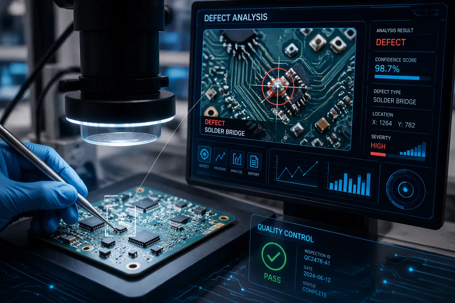
Effective PCB defect analysis uses visual checks, automated optical inspection (AOI), X-ray, and AI-based detection. You need this mix because PCB defects cause up to 30% of manufacturing scrap costs. Each detection method has different strengths. X-ray finds hidden joints. AI tools get better over time. Your PCB quality depends on picking the right tools. Every PCB defect you miss lowers your performance metrics. Printed circuit boards need careful checking at each stage. Printed circuit boards also need steady process control. You must study each defect to find its root cause. This defect analysis leads to targeted fixes. Your detection plan should measure both accuracy and speed. Poor results in either area raise defect rates. Reliable PCB detection needs proper lighting. Automated PCB detection systems need calibration.
Key Takeaways
Use a mix of visual checks, AOI, X-ray, and AI to catch different PCB defects.
Most assembly failures are caused by common defects like opens and component shift.
Design for Manufacturing (DFM) rules stop many defects before production starts.
Track numbers like first-pass yield and defect rates to see how much quality has improved.
Make sure that what you find during checks leads to changes in how you make things, so you can keep getting better.
Common PCB Assembly Defects
Before you fix any PCB assembly issues, you need to know what to look for. Understanding common PCB assembly defects helps you focus your detection efforts. This PCB defect analysis starts with recognizing frequent problems. Each defect has a specific root cause. Knowing these causes improves your accuracy in finding the real problem. Your performance in quality control depends on this knowledge.
Soldering Defects
Solder bridging creates a short circuit between two pads or pins. Excess solder paste causes this problem. Pads that are too close together also contribute. A bridge damages components and compromises reliability. On high-density PCB designs, this risk increases. Detection of bridges requires careful visual inspection or AOI. Your PCB assembly process must control paste volume for good accuracy.
Tombstoning lifts one end of a small component during reflow. Uneven heating creates this imbalance. One pad reaches melting temperature before the other. The solder on the heated pad pulls the component upward. Unequal pad sizes also cause this problem. Proper reflow profiling prevents many soldering defects. Soldering defects like voids trap gas bubbles inside the joint. You cannot see them externally. They weaken the connection and reduce performance.
Head-in-pillow affects BGA components. The solder ball and pad melt but do not merge. This creates a weak joint that passes tests but fails later. Detection of these hidden defects requires X-ray inspection. Opens account for 34 percent of PCB assembly defects. No bonding exists between the lead and pad. This creates an open circuit. Detection methods like AOI find these defects with good accuracy.
Component and Board-Level Defects
Component shift causes misalignment during reflow. Components float on molten solder. They move from their target position. This accounts for 15 percent of PCB assembly issues. Shifted parts cause shorts or opens. Lifted pads occur when the copper detaches from the board. Thermal stress above 250 degrees Celsius during reflow weakens the bond. Handling the board too soon after soldering also lifts pads. On single-sided printed circuit boards, this is more common.
Missing components stop the PCB from working. The pick-and-place machine may skip a part. Incorrect placement also leads to PCB assembly issues. Each defect you find during detection gives you data for improvement. Your accuracy in recognizing defects directly affects your performance metrics. The more you understand about PCB assembly defects, the better your PCB defect analysis becomes. Good detection of these PCB issues is the foundation of quality improvement. Reliable printed circuit boards require careful detection at every stage. Your performance in detection drives your overall quality results. Your PCB quality depends on consistent detection and analysis. Finding every defect early improves your accuracy and performance. Each defect you catch builds your knowledge.
Core Methods for PCB Defect Analysis
You need good ways to find PCB problems before customers get them. Each method has a different job in your PCB defect analysis work. The tools you pick affect how well you find defects and how your quality scores look.
Traditional Inspection Techniques
Visual inspection is the first step. You check boards under good light to see big soldering defects like bridges or missing parts. This works for clear issues but misses small problems. Your eyes get tired fast, and different inspectors see things differently.
Automated optical inspection (AOI) helps you find defects much better. High-resolution cameras scan the board in a set pattern. You compare images to design rules or a good reference board. AOI is great at spotting surface-level PCB defects like tombstoning, moved parts, and solder bridges. Machine vision in this group splits into image processing, machine learning, and deep learning. Each level adds more skill to your PCB defect detection.
X-ray inspection shows what you cannot see from the outside. Hidden solder joints under BGA parts need this tool. You spot voids, head-in-pillow defects, and poor wetting using X-ray images. But this method has limits. Good 3D CT systems cost over $100,000, and detailed scans take several minutes per board, slowing down work. You need trained workers to read results. 2D images can mix up voids with shadows from parts that overlap. Radiation safety needs controlled areas, which adds extra work. For high-reliability jobs, 3D CT is needed even though it takes time and costs money.
Microsection analysis gives the deepest look of all traditional inspections. You cut a thin slice through the board and look at it under a microscope. This destructive method shows inside PCB structures, so you can find hidden flaws like thin plating or layers that do not line up. You check that parts meet exact specs using this method. Costs are high: special tools, skilled workers, and slow turnaround times. Complex boards with many layers make this analysis harder. Yet microsection analysis gives very useful details about how the board was made. These findings help find defects and guide design changes to make manufacturing easier.
Advanced AI-Based PCB Defect Detection
Old rule-based systems struggle as PCB boards get more complex. Many layers and tight connections overload preset rules. AI-based computer vision systems, trained on many different examples, adjust and give steady results across different PCB types, from single-layer boards to complex multi-layer ones.
Deep learning models change how you find PCB defects. Models like SCMEO-DETR improve finding defects and sorting them at the same time. You tune these models on your specific defect types, getting past the limits of fixed rules. Studies show that AI-powered AOI systems can find up to 99% of defects, beating manual checks and rule-based machine vision on complex boards with parts on both sides.
Capability | Traditional Machine Vision | AI-Based Detection |
|---|---|---|
Complex defect identification | Struggles with small or hidden defects | Finds complex defects with better accuracy |
Adaptability to design changes | Needs manual reprogramming | Adjusts on its own to new designs |
False positive rate | Higher due to fixed rule limits | Lower thanks to smart pattern recognition |
Inspection accuracy | Limited by preset rules | Keeps getting better with more training data |
You check your detection results using standard scores. Precision tells you how many items marked as bad are truly bad. Recall tracks how many truly bad items were found. The F1 score combines both into one number. Average precision adds up across ten IoU levels from 50 to 95 percent. Mean average precision averages this across all defect types. Frames per second measures how fast you detect in real time. A confusion matrix shows true positives, false positives, true negatives, and false negatives for each category.
As PCB boards get more complex with many layers and tight connections, old inspection methods have a hard time keeping up. AI-based computer vision systems, trained on many different examples, adjust and give steady results across different PCB types.
These advanced methods directly help your industrial PCB defect detection goals. You learn to diagnose PCB problems step by step rather than guessing. Your detection accuracy gets better with each training round. This knowledge prepares you for the quality improvement solutions that come next.
PCB Quality Improvement Solutions
You cannot fix what you cannot measure. Quality improvement starts with design choices that stop defects before you make the board. Then you add process controls that catch problems early. Each solution below targets the root causes from your PCB defect analysis.
Design for Manufacturing (DFM)
DFM rules stop PCB assembly defects before they start. Acid traps happen when etchant gathers in tight copper corners. This causes too much etching and weakens connections. Route traces at 45-degree angles instead of 90 degrees. This small change stops chemical pooling. Your PCB layout should also follow IPC-7351 guidelines for surface mount land patterns. Check every footprint against the component datasheet. A wrong pad size causes tombstoning or poor wetting.
Thermal imbalance causes many soldering defects. When you connect surface mount pads to large copper planes, use thermal relief spokes. These spokes slow heat flow so both pads reach melting temperature at the same time. This stops tombstoning. Component clearance matters too. Leave 3-5mm board edge clearance for handling. Follow manufacturer recommendations for component-to-component spacing. Make sure pick-and-place nozzles can reach every part. Polarity indicators must stay visible after placement. Clear silkscreen marks prevent orientation errors.
Check for 'Acid Traps' (sharp angles in traces) that could trap chemicals during etching.
These design rules directly cut your defect rate. Fewer design flaws mean fewer PCB assembly issues later. Your detection systems work better when the board design follows proven patterns.
Process Controls and Testing Services
Solder paste inspection (SPI) catches problems before component placement. SPI measures volume, height, area, and alignment of each paste deposit. According to SMT Today, as much as 30% of PCB assembly defects come from solder-paste printing errors. Another study shows 64% of SMT assembly defects come from poor paste printing. SPI finds too little paste that causes weak joints. It finds too much paste that creates bridges. It spots misalignment before placement. This early detection stops costly rework.
Defect Type | How SPI Prevents It |
|---|---|
Insufficient Paste | Finds too little solder paste, stopping weak or open solder joints |
Excessive Paste | Finds too much solder paste, stopping bridging and short circuits |
Misalignment | Finds off-center paste, stopping poor component placement |
Tombstoning | Finds uneven paste application, stopping component lifting |
Reflow profile optimization fixes thermal defects. IPC-7530B gives updated profiling guidelines. Preheat ramp rates should stay below 3°C/s, best at 1-2°C/s. Soak time usually runs 60-120 seconds between 150-180°C. Peak temperature ranges 235-245°C with time above liquidus of 45-90 seconds. Cooling rates of 3-6°C/s stop too much intermetallic growth. A bad profile causes up to 90% of thermal defects. One client with a dense IoT board had a 12% failure rate from cracked capacitors. After reprogramming the oven from 3.5°C/s to 1.5°C/s ramp, the defect rate dropped to 0.1% on the next 500-unit run.
Cleaning procedures remove flux residues that cause corrosion and leakage currents. Advanced testing services add another layer of protection. HATS² technology simulates multiple convection reflow cycles up to 260°C. High-speed in-situ resistance measurements find cracks in via structures. This testing supports IPC-2221B Type D coupons. You find via structure issues before adding components. Counterfeit detection uses visual checks, X-ray inspection, XRF analysis, and decapping methods. These steps verify part authenticity and RoHS compliance.
Track your improvement with measurable KPIs. First-pass yield should reach 97-98% for standard boards. Defect rates should stay below 500 PPM. Process capability index (Cpk) should measure at least 1.33. These numbers confirm your PCB defect detection accuracy and overall performance. Your detection accuracy gets better as you refine each process step. Each control point sends data back into your quality system. This creates measurable performance gains across every production run.
Integrating Analysis with Continuous Improvement
Your work to find PCB defects does not stop when you spot a problem. The real value comes from using that information to improve your production system. This closed-loop method turns every detection into a chance to learn. You build a cycle that keeps lowering defects and boosting your results.
Closing the Loop with Data Feedback
Start by writing down every issue you find during checks and tests. Record the type, place, and seriousness of each defect. This data becomes your guide for making things better. You study the data with tools like histograms, control charts, and Pareto charts. These tools show patterns that point to specific root causes.
Once you know the source, you share the findings with your engineering teams. They look at the risks and decide which fixes matter most. Design changes and process fixes come from this analysis. Then you check that your changes work by testing and watching closely. This step makes sure your fixes stop the problem from coming back, not just cover it up.
Your AOI systems give useful data that you can use early in the design phase. Bad pad designs, trace spacing issues, and wrong footprints show up in AOI reports. Acting on this feedback helps you improve layouts before making many boards. Studies show deep learning can find defects with up to 99.4 percent accuracy. This precision lets you make targeted fixes that cut down on repeat problems.
Building a Culture of Quality
Working together across teams really improves your PCB defect detection. When feedback loops between hardware and software teams are broken, it causes compatibility issues and extra work. If test results don't reach design teams, errors stay in final products. Getting engineering involved early uncovers manufacturing problems before they turn into costly mistakes.
Shared goals shift discussions from guesses to real results. You bring every team together around clear targets like defect rates and manufacturing yield. A clear decision-making process with someone in charge prevents mix-ups and cuts down on errors from bad communication. Regular reviews of AOI reports keep everyone focused on getting better.
Training programs cut down on operator mistakes and make your team more consistent. Classes like "PCB Design for Manufacturability" teach skills that stop design issues before making boards. "Troubleshooting and Defect Analysis for Electronics Assembly" helps your team find and fix production defects quickly. In-house IPC training keeps your staff up to date when standards change. These learning investments directly boost your detection performance and overall quality numbers.
Your PCB quality depends on this repeating cycle. Analysis alone cannot solve problems. You must combine detection with fixes and ongoing learning. This data-driven cycle leads to big gains through small steps forward. Your skill at finding PCB problems grows stronger with every feedback loop you close.
Effective PCB defect analysis never ends with finding problems. You must translate every detection into targeted quality improvements. This progression matters: you identify assembly defects, diagnose them with analysis methods, apply fixes, then refine through feedback. Each step builds your PCB defect detection capability.
Your detection accuracy improves when you close the loop between findings and process changes. Every defect you catch teaches your system something valuable. Your performance metrics rise as you repeat this cycle. Analysis alone cannot reduce scrap costs. You need iterative, data-driven solutions that prevent recurring issues.
As smart manufacturing and AI tools become more embedded, the line between detection and correction will blur, enabling near-zero defect production.
FAQ
How much does PCB defect detection cost?
You can begin with visual checks and simple AOI machines for small budgets. Fancy X-ray machines cost more than $100,000. AI detection software also needs money for training over time. How much you spend depends on how many boards you make and how reliable they need to be. Start with the method that fixes your most common defect types first.
Which PCB defects appear most often?
Opens make up 34 percent of assembly defects. Component shift causes 15 percent of problems. Solder paste printing errors cause 64 percent of SMT assembly defects. You should focus on finding these common problems first. Your defect analysis data will show which issues matter most for your production line.
How does AI improve detection accuracy?
AI systems find up to 99 percent of defects on complex boards. Old rule-based systems have trouble with close connections and many layers. You train AI models on your own defect examples. This training keeps making detection accuracy better. Your false positive rates go down as the model learns your board designs.
What performance metrics should I track?
Watch first-pass yield, aiming for 97‑98 percent on normal boards. Keep defect rates below 500 PPM. Measure process capability index at 1.33 or more. These numbers show your detection accuracy and overall quality. Check them often to make sure your changes work.
How quickly can I see quality improvements?
You can see clear gains within one production cycle after making fixes. One company cut cracked capacitor failures from 12 percent to 0.1 percent after changing reflow settings. Your timeline depends on how fast you connect detection results to process changes.
See Also
Mastering Quality Control In PCB Manufacturing Processes
Common PCB Design Issues And Solutions For SMT Processing
The Complete Guide To The PCB Manufacturing Process
How To Reverse Engineer A Circuit Board Effectively
Seven Key Quality Control Steps For Heavy Copper Automotive PCBs
