Avoid These 5 PCB Design Mistakes That Cause Scrap
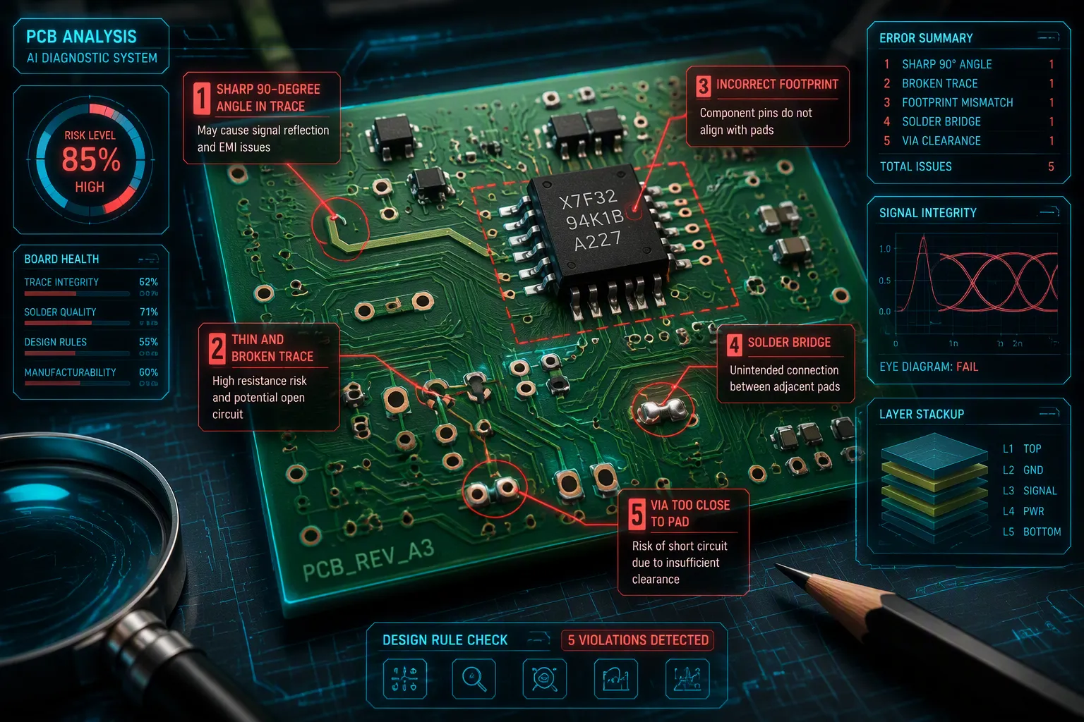
A single batch of scrapped printed circuit boards can cost thousands in materials and lost time. You can prevent most of this waste. The root cause usually traces back to recurring pcb design errors.
These design mistakes include trace spacing, impedance control, copper balancing, via design, and layer alignment. Missing test points or fiducials also create common dfm issues that manufacturers catch too late.
You can fix every one of these common pcb dfm pitfalls before fabrication. Run a dfm review early. Apply dfm rules consistently. Applying design for manufacturability principles in your pcb design process improves quality and manufacturability. This pcb dfm optimization approach reduces failures and scrap dramatically.
This guide shows you actionable solutions for each mistake. Your pcb design quality directly impacts production success. Better design-for-manufacturability practices prevent costly rework.
Key Takeaways
Make sure to follow the minimum spacing rules to avoid acid traps and short circuits.
Calculate and set the impedance early to stop signal reflections.
Use copper thieving to even out copper density and stop warping.
Make the board size and part placement better to stop drill bits from breaking and barrel cracks from forming.
Design for layer-to-layer tolerance to prevent misalignment and open circuits.
Design Mistake: Trace Spacing Errors
The Problem: Acid Traps and Short Circuits
Traces that are too close together are a top reason PCB batches fail. When copper parts sit too near each other, the etching process makes acid traps. These traps cause flaws that often ruin whole boards.
Acid traps show up in a few clear cases:
Acute angle traces: When traces meet at angles under 90 degrees, etchant pools in the sharp corners. This pooled acid corrodes copper locally, creating open circuits or shorts.
Minimal gaps between pads, traces, and vias: Narrow spaces allow acid to seep between conductors. During etching, traces can even fuse together, directly causing short circuits.
Isolated copper islands: Unused copper areas trap etchant. The acid later seeps out to damage adjacent circuitry, creating unintended connections.
System errors: Design software can inadvertently create acute angles or insufficient gaps, which become acid traps leading to the same corrosion and short-circuit failures.
Even one or two small spacing errors can scrap an entire order. Thin traces also suffer from overheating and voltage drops, compounding the problem. These failures increase scrap rates and drive up production costs unnecessarily.
The Solution: Adhere to Minimum Spacing Rules
You can prevent these defects by following your manufacturer's DFM rules from the start. Every fabricator publishes minimum spacing requirements. Apply these design rules consistently throughout your pcb layout.
The IPC-2221 standard provides baseline spacing guidelines based on voltage:
Voltage Range (V) | Minimum Spacing (mm) |
|---|---|
Vpeak < 15 | 0.13 |
15 ≤ Vpeak < 30 | 0.25 |
30 ≤ Vpeak < 100 | 0.1 + (0.01 * Vpeak) |
100 ≤ Vpeak | 0.6 + (0.005 * Vpeak) |
These values assume standard conditions. Higher voltages or harsh environments like humidity require greater clearance. Your pcb design quality depends on respecting these limits.
For pcb routing dfm, follow these practical rules:
Route traces at 45-degree angles or use smooth curves. Never create acute angles.
Eliminate V-shaped junctions where copper meets a plane. Use proper teardrops or thermal reliefs.
Check anti-pad clearance to prevent plane-to-trace shorts.
Run a design rule check before submission. This pcb dfm optimization step catches design rule violations early, reducing rework and improving manufacturability. Your component spacing decisions directly affect yield. Investing time in pcb routing dfm review costs far less than scrapping a production run. Good design rules protect your quality and your budget.
Impedance Control Failures
The Problem: Signal Integrity and Reflection Issues
High-speed circuits need exact impedance control. Many engineers miss this common design mistake. If your trace width or dielectric thickness is wrong, impedance mismatches happen. These mismatches cause signal reflections.
Reflection occurs when an electromagnetic wave hits a boundary where impedance changes. Part of the signal passes through. The rest bounces back toward the source. This leads to signal integrity issues like distortion, noise, and data errors.
Scenario | Cause of Reflection | Observed Effect |
|---|---|---|
Out-of-phase reflection | Load termination resistance lower than source and line impedance | Signal reflected 180 degrees out of phase, creating a negative voltage |
Non-uniform impedance profile | Change in trace width, loss of reference plane, or vias along the line | A series of signal reflections along the line |
Unmatched transmission line | Mismatch between transmitter, receiver, and line impedance | Complete signal distortion and voltage oscillation |
A trace with an impedance break can create reflections. These reflections lower your signal quality. In bad cases, the board fails completely. Poor connections between parts make these failures worse.
The Solution: Calculate and Specify Impedance Early
You must calculate your target impedance during the pcb design phase. Many tools exist for this task. The choice depends on your accuracy needs. This is a critical part of pcb routing dfm.
Field solvers solve Maxwell's equations using boundary conditions of your geometry. They calculate inductance and capacitance per length. From these values, they determine characteristic impedance. Field solvers handle complex shapes like asymmetrical stripline with different dielectrics. They achieve accuracy better than 1%.
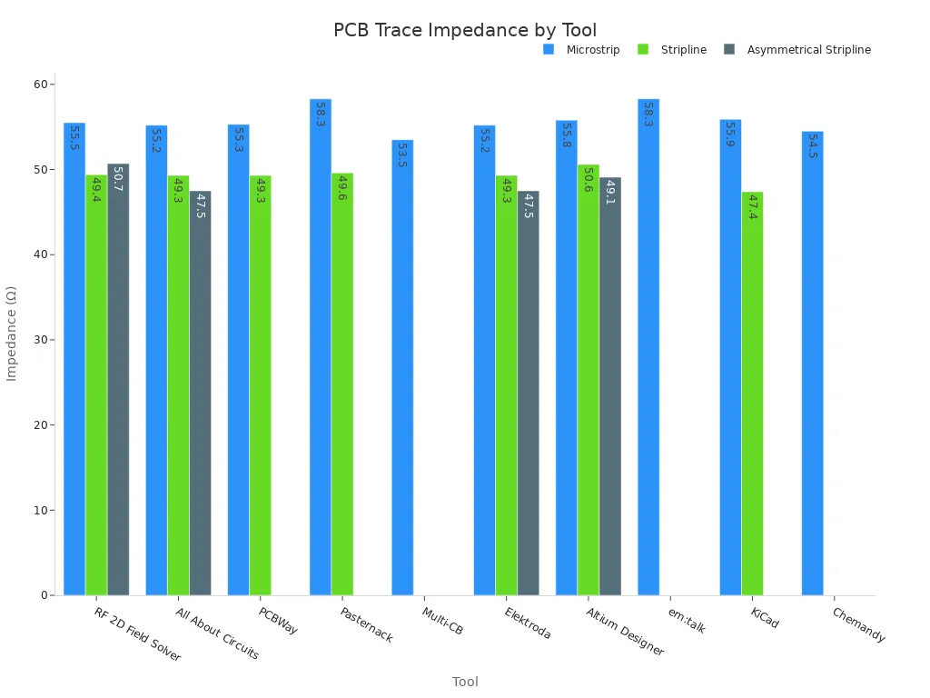
Online calculators use closed-form equations. They offer accuracy within 5-10%. EDA tools provide convenience but may lack advanced modeling. For critical pcb designs, use a dedicated field solver.
After calculation, specify your impedance in the fabrication notes. Include the target impedance, trace width, trace height, and Z-axis distance to the reference plane. For differential traces, include copper-to-copper spacing. Use a clear format. This is a key dfm practice.
Standard impedance tolerance is ±10%. Tighter tolerances like ±5% increase cost and scrap rates. Only specify tighter tolerances when your circuit needs them. Ensure your notes and stack-up view are consistent. Conflicting information delays your order. Follow these design rules carefully.
This pcb dfm optimization step prevents expensive rework. Good pcb routing dfm practices include impedance planning from the start. Your pcb design quality improves when you address impedance early. These design rules protect your signal integrity and reduce failures. Better manufacturability starts with accurate impedance specifications.
Inadequate Copper Balancing
The Problem: Panel Warpage and Plating Defects
When copper is spread unevenly across your layers, it causes big problems. During lamination, areas with more copper heat up and cool down at different rates than areas with less copper. Copper expands at about 17 ppm/°C, while FR-4 expands at 14-16 ppm/°C. This difference adds stress when one layer holds 90-95% copper and the opposite layer holds only 20-40%. The board bends toward the side with less copper.
You can see this clearly in RF boards. One layer has a large ground plane. The opposite layer has few traces. After pressing, the board warps toward the signal side. Power and signal hybrid boards show the same problem.
These imbalances also cause plating defects. Uneven current distribution creates voids in the copper plating. You also get weak solder joints. The board fails during assembly. These failures raise scrap rates. Catching these design mistakes early prevents costly rework.
The Solution: Use Copper Thieving and Symmetry
You can fix these issues with copper thieving. This method adds non-functional copper patterns to areas with little copper. These patterns look like dots, squares, or crosshatch. They have no electrical connection. Their only job is to balance copper density. During electroplating, current flows toward isolated copper features. This spreads current density evenly. You get uniform copper thickness.
Without copper thieving, plating thickness varies by 20-30% across the panel. With thieving, that variation drops below 10%. Board warpage improves from 1.0-1.5% bow/twist to less than 0.5%. Aim for 40-60% copper density per layer. Keep density variation under 15-20%.
Thieving also controls resin flow during lamination. It prevents excess resin buildup. This reduces voids between layers. Thieving patterns spread heat evenly. The board expands and contracts uniformly.
Board warpage from asymmetric stackup: Mechanical stability is as vital as electrical performance. Warpage happens when thermal expansion forces are unbalanced. Copper weight must mirror about the center axis.
For best results, plan your stackup early. Mirror copper distribution on both sides of the board's centerline. In an 8-layer board, if layer 1 has dense copper, layer 8 should have similar density. Check your pcb layout with the manufacturer. Follow IPC-6012 guidelines. Your pcb routing dfm practices prevent issues and reduce scrap.
Following these design rules improves your pcb design quality. Good pcb dfm optimization starts with copper balancing. Your pcb design also benefits from planning. These design rules protect your budget and improve overall quality. Apply these pcb design principles consistently. The pcb passes through fewer cycles. Your boards have better manufacturability and higher yield.
Poor Via Design Choices
The Problem: Drill Breakage and Barrel Cracks
Small vias can cause drill bits to break. If the via is too small, the drill bit faces uneven pressure. Vias placed too close to the board edge create the same issue. The bit cuts through material and air unevenly. This leads to misalignment and breakage.
Short slots are hard to drill in PCBs. The slot length should be at least 2.5 times its width.
Short slots are the hardest to drill in PCB manufacturing. A short slot has a length less than twice its width. When drilling the start and end points, the drill bit sits partly on the board and partly in open air. This creates uneven forces, causing misaligned or shortened slots. For best results, design slots with a length-to-width ratio of 2.5 or higher.
Barrel cracks happen because materials expand at different rates. Dielectric materials grow more than copper when heated. This puts stress on the via barrel. Thermal cycling makes cracks worse. Thin copper plating cannot absorb much stress. Plating voids weaken the barrel too. High aspect ratio vias plate unevenly. Dense via-in-pad and large copper planes raise crack risk. Poor drilling adds to the problem. These issues cause open circuits and weak connections. Such failures increase scrap and lower product quality.
The Solution: Optimize Via Size and Placement
Your pcb design should use proper via sizes. Follow these aspect ratio rules. Through-hole vias work best between 6:1 and 10:1. Laser-drilled vias need a ratio of 1:1 or less.
Via Type | Typical Aspect Ratio |
|---|---|
Standard through-hole | 6:1 to 8:1 |
Advanced through-hole | Up to 10:1 |
High-control through-hole | Up to 12:1 (requires engineering review) |
Laser microvia | 0.75:1 to 1:1 |
Stacked microvias | Approximately 1:1 per layer |
Add proper annular rings. Keep the minimum width at 0.15 mm. This ensures the copper ring surrounds the drilled hole. Use tenting or plugging for via protection. Only tent vias with a diameter of 0.3 mm or smaller. Larger vias require plugging. Set the solder mask expansion to zero or negative in your CAD software.
Tenting stops solder from wicking during assembly. Solder wicking pulls solder away from pads. This creates soldering defects and voids in the barrel. Plugging fills the via completely. This prevents voids and improves solder quality. Verify plugging fill by X-ray inspection. Specify tenting requirements in your assembly notes.
Use these dfm design rules to improve your pcb design quality. Good pcb design and pcb dfm optimization start with via planning. Your boards will have fewer defects and better manufacturability. This reduces scrap.
Pcb Design Mistake: Misaligned Layers
The Problem: Registration Errors and Open Circuits
Layer misalignment happens when the maker cannot line up all copper layers perfectly. Each layer must match the others within tight limits. When layers shift, pads no longer line up with their vias. Open circuits show up where connections should be.
Fine line designs suffer the most. These boards use narrow traces and small pads. Even a tiny shift causes a full failure. A pad that moves by a tiny amount may miss its via completely. The board cannot work. You throw away the whole batch.
Registration errors also cause misaligned solder pads. Components cannot attach the right way. Assembly workers find the problem late. They waste time and materials. These failures raise your production costs. Your pcb design quality drops.
The Solution: Design for Layer-to-Layer Tolerance
You can stop these issues with careful planning. Start with a balanced stack-up. A balanced layer structure lowers stress during lamination. The board stays flat. Layers stay aligned.
Add fiducials to your design. These are small copper marks that help the maker align layers. Put them on the board edge and near key components. The machine uses them as reference points. This boosts registration accuracy a lot.
Check your maker's registration ability before finishing your layout. Each fabricator has different tools. Some hit tighter limits than others. Ask for their capability data. Design your pads and vias to fit within their limits. This is a key dfm practice.
Your pcb design should also account for material movement. Different materials expand at different rates. Your maker can advise on expected movement. Use their guidance when setting your design rules.
Run a dfm review before sending. This pcb dfm optimization step catches possible alignment issues early. You can adjust your layout before making starts. This saves time and money.
Good design rules protect your manufacturability. Your boards will have fewer defects. Your connections will work reliably. Your pcb design quality improves with each review cycle. Apply these principles consistently. Your production runs will go smoother. Your scrap rates will drop.
These five mistakes share one root cause: you did not look ahead to manufacturing. Trace spacing, impedance, copper balance, vias, and layer alignment all need early planning. Each one creates scrap when ignored.
Investing time in dfm review costs far less than replacing failed boards. A thorough design for manufacturability check catches common pcb dfm pitfalls before fabrication begins. This pcb dfm optimization step protects your budget and your schedule.
Use this list as your pre-submission checklist. Verify each point before sending files. Your pcb design quality improves with every review. Fewer failures mean smoother production runs. Better pcb design leads to reliable products you can ship with confidence.
FAQ
What is the most common cause of PCB scrap?
Traces that are too close together cause acid traps during etching. These traps lead to shorts and open circuits. Follow your manufacturer's minimum spacing rules. Run a design rule check before sending your files.
How does copper thieving improve board quality?
Copper thieving evens out copper density across layers. This stops panel warpage and cuts down on plating voids. You get even copper thickness. Board quality improves with fewer defects.
What failures come from ignoring impedance control?
Impedance mismatches cause signal reflections. These reflections lead to data errors and signal distortion. Your board may fail completely. Specify target impedance in your fabrication notes to avoid these failures.
How can you prevent soldering defects from via design?
Tent or plug your vias to stop solder wicking. Use proper annular rings. Follow aspect ratio rules for your via type. These steps improve solder quality and reduce assembly defects and voids.
What is the best way to start a dfm review?
Review your manufacturer's design rules first. Check trace spacing, copper balance, via sizes, and layer alignment. Use this blog's checklist. This pcb dfm optimization step catches issues before fabrication starts.
See Also
Ten Proven Methods To Reduce Custom PCB Fabrication Costs
Essential Precautions To Follow In PCB Circuit Board Design
Frequent Issues And Fixes In PCB Design For SMT Assembly
Seven Steps For High Current Heavy Copper PCB Quality Control
