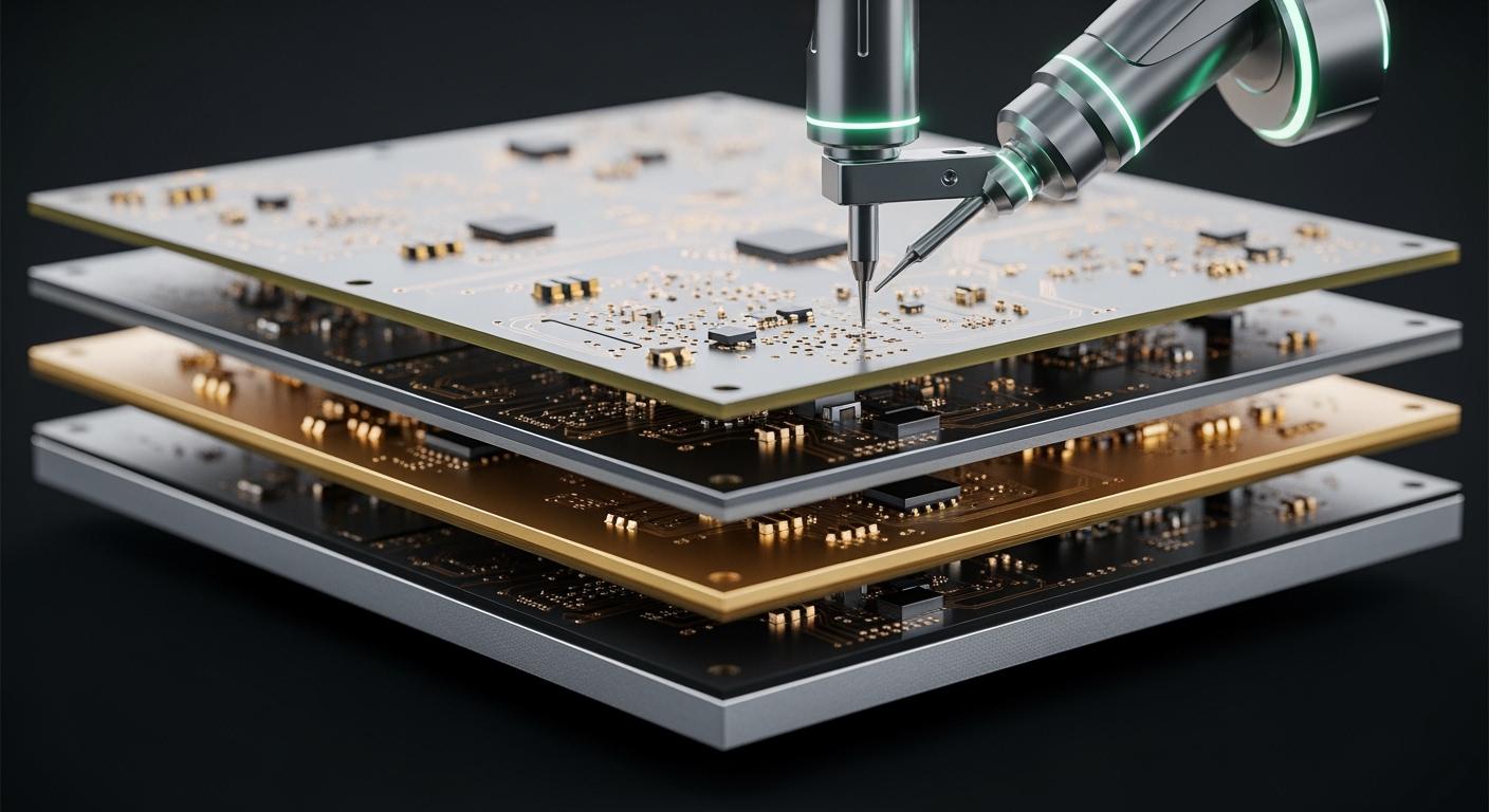
Multi-layer PCB Alignment Control Design Techniques
You must watch pcb alignment control in multilayer pcb design. Small mistakes in alignment can make signals weak or cause short circuits. These mistakes can even make the board stop working. If you use old methods like fiducials and tooling holes, you help pcb alignment control. Newer systems like optical imaging give you better accuracy. The effect of pcb layering gets bigger with each new signal or power layer you add. Good pcb alignment control keeps your fast and complex design working well. Think about alignment control from your very first design step.
Key Takeaways
Good alignment control is very important in multilayer PCB design. It helps stop signal loss and circuit problems.
Some common alignment problems are missing fiducials and wrong pad sizes. These mistakes can cause expensive errors during production.
Use optical alignment systems to make accuracy better. Always check with other ways to make sure it is reliable.
Add fiducials and tooling holes in your design. This helps line up layers and makes manufacturing faster and easier.
Think about alignment at the start of your design. This helps stop problems and makes your multilayer PCBs strong and reliable.
Multilayer PCB Alignment Challenges
Common Misalignment Issues
Working with multilayer pcb designs is hard. Problems with inter-layer alignment can happen anytime. These problems can waste time and money. The most common issues are missing fiducials, bad stencil design, and wrong pad sizes. These problems make it hard to line up layers.
Here is a table that lists the most common misalignment problems in multilayer pcb fabrication:
Misalignment Issue | Description | Impact |
|---|---|---|
Missing or Misplaced Fiducials | Automated systems need fiducials. If they are missing, boards get misaligned and more boards are thrown away. | Example: 12% of boards are wasted, costing $42,000, when fiducials are left out. |
Inadequate Component Clearance | Not enough space can cause solder to bridge and parts to touch. | 28% of SMT problems come from not enough space, costing $0.75 to fix each bad board. |
Incorrect Pad Dimensions | Wrong pad sizes can cause tombstoning and weak solder joints. | Using old pad libraries can make boards fail when stressed. |
Poor Stencil Design | Wrong stencil holes give too much or too little solder. | Solder paste problems cause 35% of SMT assembly failures. |
You need to watch inter-layer alignment when stacking layers in high-density multi-layer pcbs. Even a tiny shift can cause problems in every layer.
Effects on Performance and Reliability
Misalignment in multilayer pcb designs is not just an assembly problem. It can also hurt how your board works. Errors in inter-layer alignment can cause signal reflection, signal loss, and crosstalk. These problems make circuits less reliable.
Here is a table that shows how misalignment can hurt electrical performance:
Problem Type | Description |
|---|---|
Signal Reflection | If impedance does not match, some signal bounces back. This can cause errors or noise. |
Signal Loss | Too much signal fades away, making it weak over distance. |
Crosstalk | Electromagnetic interference can mess up data if impedance is not controlled between nearby traces. |
If you do not control inter-layer alignment, you can have long-term failures. Bad alignment can make your board weaker. It can cause layers to peel apart and open circuits. The table below shows the risks:
Impact Area | Potential Risk |
|---|---|
Mechanical Strength | Layers may not stick together and can peel apart |
Electrical Performance | Impedance can change and signals can be lost |
Thermal Reliability | More likely to crack when heated or cooled |
Long-Term Reliability | Boards can fail more often in tough conditions |
Tip: Always check inter-layer alignment at every step. This helps you avoid mistakes and keeps your multilayer pcb working well.
Essential PCB Alignment Control Techniques
Optical Alignment and Imaging Systems
You can use optical alignment systems to make multilayer pcb manufacturing more accurate. These systems have cameras that look for alignment marks on each layer. The cameras help keep layers in the right place during advanced pcb layering. When you use cameras, you make fewer mistakes. This gives you better layer registration, which is important for high-density boards.
Some optical systems use CCD technology and can be very precise. They can line up layers as close as ±3 micrometers. This is important for advanced pcb layering, especially with complex multi-layer pcb design. You can check where each layer is before you press them together. This helps you stop mistakes that could cause problems later.
But, optical alignment systems have some limits. High-density interconnects need very high accuracy, sometimes less than 50 micrometers. Small mistakes at the start can get worse as you add more layers. Changes in the material, like shrinking or uneven pressure, can also make alignment harder. Sometimes, optical systems cannot see features that are buried inside, so fixing problems right away is tough.
Here is a table that shows some common limits of optical alignment systems:
Limitation Type | Description |
|---|---|
Alignment Accuracy | Hard to reach sub-50 micrometer accuracy for high-density multilayer pcb applications. |
Cumulative Errors | Small mistakes can add up as you stack more layers. |
Material Variations | Shrinkage and pressure changes can cause alignment problems. |
Inspection Limits | Hard to measure buried vias and features during advanced pcb layering solutions. |
You can get better results by using optical alignment with other methods. Always check for changes in the material and handle panels gently to avoid mistakes.
Tip: Use optical alignment for advanced pcb layering, but always check with other tools for the best results.
Fiducials, Tooling Holes, and Labeling
Fiducials and tooling holes are old tools that help keep layers in the right place during multilayer pcb assembly. Fiducials are marks you put on the board as reference points. These marks help machines line up each layer during advanced pcb layering solutions. You should use at least three fiducials on each side for global alignment. For small parts, local fiducials stop shorts and help with accuracy.
Tooling holes give you a fixed spot to hold and move the board during manufacturing. They help you make fewer mistakes and speed up the process. Tooling holes also help machines work better, which is important for optimization in big production runs.
Here is a table that explains the types of fiducials and what they do:
Type | Description | Role in Alignment Accuracy |
|---|---|---|
Global | Used for the whole board. At least 3 per side. | Keeps the entire multilayer pcb aligned. |
Panel (Array) | Placed on rails or waste strips. | Aligns the whole panel for consistent processing. |
Local | For fine-pitch parts like BGAs and QFPs. | Prevents shorts and keeps components accurate. |
You also need good labeling for tracking and checking alignment. Labels must follow rules like IPC-7351, UL Marking, and RoHS/REACH. These rules help you track boards and show they are safe and meet environmental laws.
Here are some best ways to label:
Use strong labels that last in the board’s environment.
Make sure labels do not get ruined by chemicals.
Design labels so they are easy to read and follow the rules.
You should also:
Show batch or lot numbers to link boards to production runs.
Add serial numbers to track each board.
Use codes that machines can read for fast data capture.
Note: Good labeling helps you optimize and find problems fast.
Layer Registration and Stacking Stripes
Layer registration means making sure each layer lines up right during advanced pcb layering. You can use stacking stripes to help with this. Stacking stripes are copper lines at the edges of the layers. The first stripe is 200 mils long and 50 mils wide. Each new layer adds 100 mils to the length. This pattern helps you see the order and direction of layers during advanced pcb layer stacking.
Stacking stripes give workers a visual guide. This lowers mistakes during lamination and helps with optimization. You can find errors before you press the layers together. This is important for making high-quality multilayer pcbs.
You should also watch prepreg and registration. Prepreg is the sticky stuff that holds layers together. If you do not control prepreg flow and registration, layers can move during lamination. Always check where each layer is before and after pressing. This helps with advanced pcb layering and keeps your boards strong.
Callout: Use stacking stripes, careful prepreg use, and regular checks for the best layer stacking results.
Implementation in Multi-layer PCB Manufacturing
Design for Alignment Control
You need to think about alignment control from the start. Planning early helps you avoid many problems later. If you focus on alignment, your board will work as it should.
If copper sheets are not lined up, the system can fail.
Wrong alignment can make contact points miss or stop current flow.
Circuits might not work if you do not plan for alignment.
Inner layer registration must be accurate for good electrical performance.
Good alignment keeps multilayer pcbs strong.
Making lots of boards for HDI, high-speed, and high-reliability needs good alignment.
Always plan your pcb stackup with alignment in mind. Put signal layers next to ground planes. This helps keep signals clear and controls impedance. It also helps stop noise. Good stackup choices make advanced pcb layering easier and more reliable.
Tip: Use clear marks like fiducials and tooling holes in your design. These help machines and people line up each layer during advanced pcb layering.
Manufacturing and Lamination Steps
You must follow careful steps in multi-layer pcb manufacturing. Each step affects the final alignment and strength of your board. The stackup must stay correct as you add layers.
Here is a step-by-step guide for alignment control in manufacturing:
Prepare Inner Layers
Print and etch each inner layer. Use advanced pcb layering tools to check patterns and alignment marks.Inspect and Register Layers
Use optical systems to check each layer. Make sure all alignment marks match. This keeps the stackup in order.Stack and Pin Layers
Stack layers in the right order. Use pins in tooling holes to hold them. Stacking stripes help you check order and direction.Apply Prepreg and Laminate
Add prepreg between layers. This sticky stuff holds the stackup together. Use even pressure and heat to bond layers. Watch for material changes, as many lamination cycles can cause big alignment errors. Each new layer can make small mistakes worse, so control the process closely.Drill and Plate Vias
Drill holes for vias using X-ray alignment. This keeps vias in the right place and protects connections between layers.Final Inspection
Check the finished stackup for shifts or defects. Use advanced pcb layering inspection tools to find problems early.
Note: Always handle panels gently and keep the environment steady. Changes in temperature or pressure can cause misalignment.
Quality Assurance and Inspection
You must check your multilayer pcb at every step to keep it strong. Quality assurance uses many tools and ways to find alignment errors before they get worse.
Quality Assurance Method | Control Aspect | Value Delivered |
|---|---|---|
Inner Layer Imaging & Dimensional Control | Image scaling compensation | Dimensional accuracy |
Tooling Hole & Registration System Control | Precision tooling holes | Reliable registration |
Lamination Process Accuracy Control | Pressure uniformity | Layer stability |
Material Selection & Stack-Up Engineering | Low-shrinkage materials | Predictable behavior |
Drilling Accuracy & Via Registration | X-ray drilling alignment | Precise via positioning |
Inspection & Verification in Mass Production | X-ray inspection | Early defect detection |
Automated optical inspection (AOI) systems are important in advanced pcb layering. These systems use cameras and software to check alignment. AOI takes pictures of your board and compares them to the design. The process uses image capture, light control, image processing, and defect finding. New AOI systems can use many viewing angles and 3D imaging for better checks. AOI gives steady accuracy and lowers mistakes that people might make.
AOI systems check if components are lined up during assembly.
They look for correct polarity indicators for part orientation.
The systems make sure parts are put in the right place as the design says.
AOI systems help keep your multilayer pcb strong. They also help signal integrity by making sure every part is in the right spot. When you use these systems, you get better results in mass production and advanced pcb layering.
Callout: Always use both manual checks and automated systems. This way, you have the best chance to find errors and keep your multi-layer pcb manufacturing strong.
By following these steps and using the right tools, you can keep your stackup strong and get better signal integrity in every multilayer pcb you make.
Best Practices for Advanced PCB Layering
Design Tips for Alignment Accuracy
You can get good alignment in multilayer pcb designs by following some easy tips. Pick a dielectric material with a low dielectric constant and dissipation factor. This helps signals stay clear and keeps delays short. Put signal layers between ground planes to block electromagnetic interference. This also gives signals a safe path back. Place microvias close to signal pads to stop impedance problems and cut down on signal reflections. Route traces carefully to keep impedance steady and stop signals from getting weak. Put decoupling capacitors near power pins to keep power strong and lower noise. For better pcb layer optimization, use process controls and QA systems. Watch temperature changes, lamination pressure, and etching limits. Use automated optical and laser registration systems that look for laser-etched fiducials. This cuts down on mistakes and makes results more repeatable.
Avoiding Common Pitfalls
You can stop common mistakes in pcb layer optimization by making via aspect ratios better. This helps plating stay even and lowers the chance of weak spots or empty spaces. Using via-in-pad and blind via setups makes routing shorter and puts less stress on stacked vias. Check stacked via alignment during design to stop misalignment that can cause problems later. Get feedback for design for manufacturability during reviews. Change layouts, make spacing better, and fix stack-ups to help with final alignment. For electronics manufacturing, check each layer for good registration and do not take shortcuts that hurt quality.
Tip: Always check your stack-up and registration marks before you finish your multilayer pcb design.
Collaboration Between Design and Fabrication
Working together helps designers and fabricators get better alignment in multilayer pcb projects. Good communication makes sure everyone follows best practices in design and making boards. Use online tools to help with design and check signal integrity with built-in calculators for trace lengths. Use thermal management tricks like thermal vias. Get feedback from fabrication services to make designs better. Give full documents, like Gerbers and BOMs, and support design reviews and DFM feedback before making the board. Keeping version control and layout history open helps everyone know what is happening. Good pcb layer optimization needs teamwork and clear documents. Layer optimization for electronics manufacturing works best when you share info and listen to feedback.
Collaboration Strategy | Benefit |
|---|---|
Complete Documentation | Fewer errors |
Design Reviews & DFM Feedback | Better manufacturability |
Version Control Transparency | Improved traceability |
Callout: You can get reliable multilayer pcb alignment by using careful design, process control, and teamwork for every layer.
Tools and Technologies for Alignment Control
Software for Alignment Verification
You can use advanced software to check alignment in multilayer PCB designs. These tools help you find mistakes before you build the board. Many programs use artificial intelligence to make your work easier and faster. Some software can predict errors and suggest better ways to place parts. Other programs run automatic checks to make sure layers line up.
Here is a table that shows popular software tools and their AI features:
Software Tool | AI Features Description |
|---|---|
Altium Designer | Uses machine learning for part placement and routing. Checks design rules and runs auto-simulations. |
Autodesk Fusion 360 | Offers AI-assisted layout, auto-routing, and signal checks. Works well for projects with both mechanical and electrical needs. |
OrCAD | Includes AI modules for better design. |
KiCAD | Supports AI plugins to boost design speed. |
Mentor Graphics | Uses AI to improve layout and reduce errors. |
These tools help you catch problems early. This saves time and stops costly mistakes.
Tip: Always run alignment checks in your design software before sending files to the factory.
Hardware and Imaging Solutions
You can use special machines to check layer alignment during PCB assembly. Automated X-ray systems look inside your board and spot problems you cannot see. These machines use smart cameras and image processing to find misalignment. They check for expansion, shrinking, or shifting between layers.
Laser Direct Imaging (LDI) is another tool that helps you get perfect alignment. LDI does not need film masks, so you avoid errors from manual setup. It can reach sub-micron accuracy and adjust for changes in the material as you build the board. This means you get tight tolerances and better results.
Here is a table that compares LDI with older methods:
Feature | Laser Direct Imaging (LDI) | Traditional Methods |
|---|---|---|
Accuracy | ±5 microns | ±25 microns |
Setup Time | Fast (digital input) | Slow (needs masks) |
Cost for Small Runs | Low | High |
Flexibility | High | Low |
Line Width Capability | 25 microns | 50 microns or more |
Modern imaging systems, like the Perfect Test system, can reach 0.001-inch accuracy. These tools help you fix problems right away and improve your board quality. When you use advanced alignment tools, you get better yield rates and fewer defects.
Note: Using the right tools makes your multilayer PCB stronger and more reliable.
You are important for making multilayer PCBs work well. When you manage layers carefully, your boards stay strong and work the same every time. You stop problems by making sure layers line up right and graphics are the right size.
Good alignment helps signals move clearly and keeps the board tough.
In jobs like aerospace, medical, and cars, good alignment stops big mistakes and keeps everyone safe.
New things like AI design, green materials, and better ways to build will help you do even more.
Keep using these smart steps to make boards that last and work better.
FAQ
What is PCB alignment control?
PCB alignment control means keeping layers in the right place. You use marks, holes, and machines to check positions. This helps your board work well and stay strong.
Why do you need fiducials in multilayer PCBs?
Fiducials help machines find the right spot for each layer. They are reference points for alignment. Without fiducials, boards can have errors and parts may not line up.
How does optical alignment improve PCB quality?
Optical alignment uses cameras to check where layers are. You get better accuracy and make fewer mistakes. This method helps boards work better and last longer.
What happens if layers are misaligned?
Misaligned layers can cause signal loss or short circuits. Connections may be weak and boards can fail tests. Good alignment stops these problems from happening.
See Also
Essential Knowledge For Designing Multi-Layer PCB Circuit Layouts
Key Process Guidelines For Multi-Impedance Control In PCB Manufacturing
Applications Of Multilayer PCBs In Various Industries
Frequent PCB Design Issues And Fixes For SMT Technology
Challenges In Manufacturing And Prototyping Multi-Layer Circuit Boards