PCB Fine Line Design
You use pcb fine line design when you need to fit many connections in a small space. This process means you create very narrow traces and spaces on a pcb. Start by choosing the right materials and design tools. Check your trace width and spacing limits. Make sure your design supports high-speed signals. Fine line pcb helps you build powerful devices like smartphones and medical equipment.
Key Takeaways
Fine line PCB design puts many connections in tight spaces. This is helpful for devices like smartphones.
Picking the correct materials and tools is very important. It helps manage signals and heat in fine line PCBs.
Fine line PCBs make signal quality better. They also let more parts fit in a small area.
Working with manufacturers helps stop defects. It also makes PCB quality better.
Using EDA tools and simulations helps design fine line PCBs well. It also helps test them in a good way.
Understanding Fine Line PCB
Fine Line PCB Standards
When you look at a fine line pcb, you notice the traces and spaces are very thin. These boards follow special rules to keep the lines small for high density pcb designs. Most companies say the smallest line width and space should be between 0.05 mm and 0.075 mm. Flexible boards use these numbers a lot, but some factories can make even smaller lines. You can see the usual standards in the table below:
Parameter | Minimum Value |
|---|---|
Minimum Line Width | 0.05 mm (50 µm) |
Minimum Line Spacing | 0.075 mm (75 µm) |
Trace Width | 5 mil (0.127 mm) |
Line Spacing | 5 mil (0.127 mm) |
Trace to Board Edge | ≥ 0.3 mm (20 mil) |
BGA Escape Routing (1 mm pitch) | 6 mil/6 mil (one trace) |
4 mil/4 mil (two traces) |
You must use these rules when you design fine pitch pcb. If you make the traces smaller, you can add more connections and parts on your pcb. This lets you build high density pcb for advanced electronics.
Why Fine Line PCB Matters
Fine line pcb gives you lots of good things. You can put more parts in a small space. This is important for things like smartphones and tablets. You also get better signal quality because smaller vias and careful layer changes stop problems and crosstalk. You can make heat move better by using special layer stacks and more copper. These things help your pcb work well in tough places.
Tip: Fine line pcb design helps you make strong devices without making them bigger.
HDI PCBs are important in pcb fine line design. You use microvias and fine-line routing to make the board smaller. Microvias are tinier than normal holes, so you save space. Blind and buried vias join layers inside the board without making it thicker. These tricks help you build tiny, light boards with high density pcb features.
Fine Line Applications
You see fine line pcb in many fields. These boards help make things smaller and support fast signals. The table below shows where fine line pcb is used most:
Industry | Application |
|---|---|
Consumer Electronics | High-precision design requirements |
Medical Devices | Miniaturization and dense component integration |
Telecommunications | Support for 5G communications |
Automotive | Advanced electronic systems |
Aerospace | High-speed signal applications |
High-Frequency Systems | Miniaturization and integration |
Smartphones | Common use in modern devices |
Advanced Computing | Support for high-speed signals |
Wearable Technology | Miniaturization and integration |
RF Systems | High-frequency applications |
You find fine line pcb in smartphones, medical devices, and car electronics. These boards let you make products with lots of connections in a small area. You also use them in high-frequency systems and wearable tech. Fine line pcb makes your designs better and more dependable.
Key Design Considerations
Material Choices
You need to pick the right materials for pcb fine line design. The material you choose affects how well your pcb handles signals, heat, and fine line control. Some materials work better for high-speed or high-frequency circuits. Others help you keep your lines thin and your board stable.
Here is a table that shows common materials and their uses:
Material Type | Key Properties | Applications |
|---|---|---|
PTFE-based laminates | Low-loss dielectric, keeps signals strong at high frequencies | High-frequency designs up to 10 GHz |
High-Tg FR-4 variants | Good thermal stability, works well for fast signals | High-speed pcb designs |
Copper foils | Smooth surface (0.5 μm RMS), less signal loss, better etching for fine line control | Fine line pcb fabrication |
You should use PTFE-based laminates if you need your board to work at very high frequencies. High-Tg FR-4 is a good choice for most fast digital circuits. Copper foils with a smooth finish help you make small trace widths and keep your lines sharp.
Tip: Always check if your material can handle the fine line control you need for your design.
Trace Width & Spacing
Trace width and spacing are very important in fine pitch pcb. You must keep your traces narrow and close together, but you also need to make sure your board works well and does not overheat. Fine line control helps you balance these needs.
Here is a table that explains the main challenges:
Challenge | Description |
|---|---|
Manufacturing Limitations | When trace widths shrink to 25-50 μm, making the board gets harder. You need very careful etching. |
Signal Integrity Risks | Narrow traces and close spacing can cause crosstalk. Try to keep spacing and width at a 1:1 ratio for low-speed signals. |
Thermal and Current Handling | Thin traces have more resistance. They can get hot. Use calculators to check if your traces can handle the current. |
You should always check the limits of your manufacturer. Use fine line control to keep your traces as small as needed, but not smaller than what your factory can make. If you make your traces too thin, your pcb may not work well or may fail.
Signal Integrity
Signal integrity means your signals stay strong and clear as they move through your pcb. Fine line control becomes more important as you make your traces smaller and closer together. You must watch out for several problems:
Crosstalk: Signals from one trace can jump to another if they are too close.
Impedance Mismatches: If your trace impedance changes, signals can bounce back and cause errors.
Signal Delay and Skew: If signals take different paths, they may not arrive at the same time.
Power Integrity Issues: Voltage drops and ground bounce can add noise to your signals.
You can use fine line control to keep your traces spaced just right. This helps you avoid crosstalk and other signal problems. Try to keep your trace paths short and direct. Use ground planes to help control noise.
Note: Good fine line control helps you keep your signals clean, even in high-density designs.
Impedance Control
Impedance control is key for high-speed and high-frequency pcb. You need to make sure your traces have the right impedance so signals do not reflect or lose strength. Fine line control lets you set the trace width, spacing, and layer stack just right.
Here is a table that shows what you need to control impedance:
Key Factor | Description |
|---|---|
Material Selection and Consistency | Use materials with a stable dielectric constant (Dk) at all frequencies and temperatures. |
Stackup Engineering and Validation | Design your layer stack with fixed dielectric thickness for steady impedance. |
Copper Thickness and Etching Control | Keep copper thickness even. Fine line control helps you get the right trace shape. |
Lamination Process Stability | Make sure the lamination process keeps the dielectric thickness and resin spread even. |
Impedance Coupon Design and Measurement | Add test coupons to your pcb. Use TDR tools to check impedance. |
Typical Controlled Impedance Tolerances | Set targets for single-ended, differential, and RF lines. |
You should talk to your manufacturer about fine line control and impedance needs. Use test coupons to check your board after it is made. This helps you make sure your pcb meets your design goals.
Tip: Fine line control is not just about making things small. It is about making your pcb work better and more reliably.
PCB Manufacturing Challenges
Manufacturing Limits
There are strict rules when you design fine pitch pcb. Manufacturers decide the smallest trace width and spacing. They base this on how thick the copper is. If you go smaller than their limits, you can get defects. You might also get fewer good boards from each batch. The table below shows the smallest sizes for different copper thicknesses:
Copper Thickness | Minimum Width | Minimum Spacing |
|---|---|---|
18um | ≥4/5 mil | ≥4/4 mil |
35um | ≥5/6 mil | ≥5/5 mil |
70um | ≥7/8 mil | ≥6/7 mil |
105um | ≥10/12 mil | ≥8/10 mil |
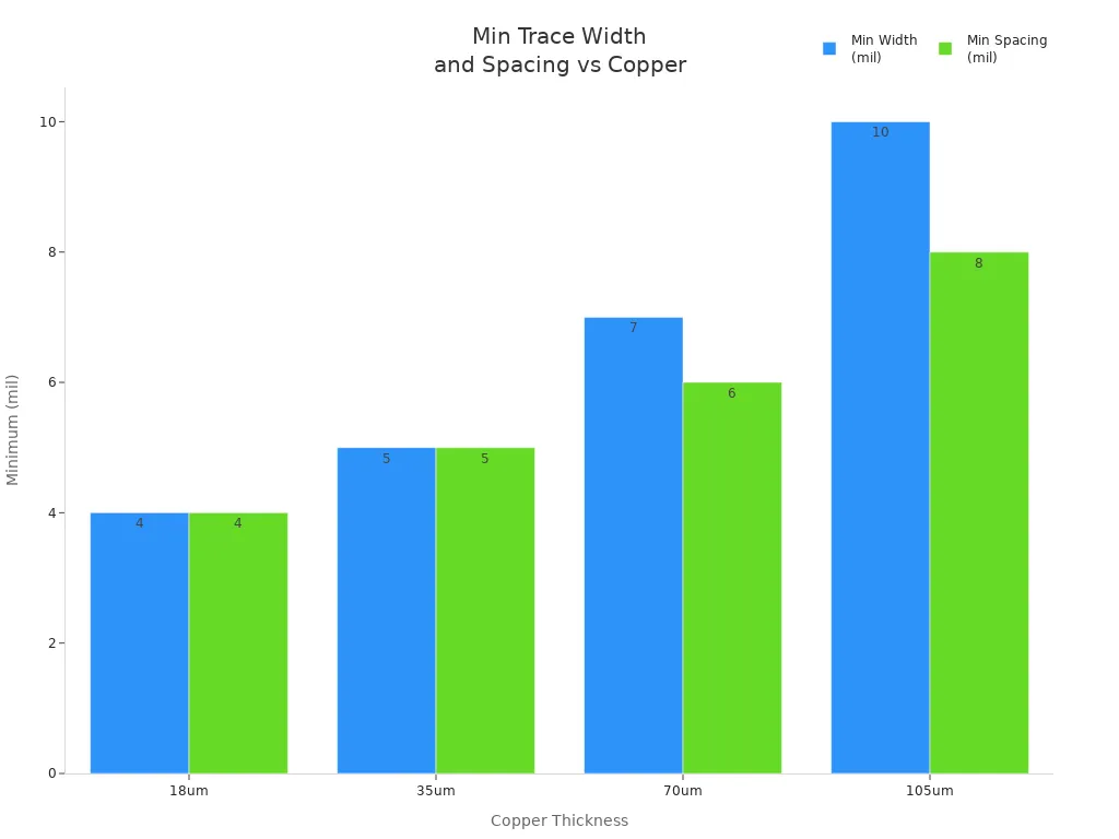
Modern pcb fine line design lets you make traces as small as 30 microns. Some factories can make lines even thinner, down to 25 microns. They use special micro PCB technology. You need to ask your manufacturer what sizes they can make.
Common Defects
You must look out for problems during manufacturing. These problems can break your pcb or make it not work. Here are the most common problems:
Plating Voids: Gaps in copper stop electricity from flowing.
Acid Traps: Sharp corners hold acid and make weak spots.
Thermal Issues: Gaps between pads and planes cause too much heat.
Insufficient Copper-to-Edge Clearance: Copper too close to the edge can short or rust.
Bow and Twist Issues: The board bends or twists, which makes building hard.
Tip: Careful design and talking with your manufacturer can stop these problems.
Manufacturer Collaboration
You get better boards when you work with your manufacturer. If you talk to them early, you get advice on your design. You also learn what they can do. Sharing your pcb design and talking about how they build helps you avoid mistakes. The table below shows why working together helps:
Evidence Description | Explanation |
|---|---|
Early engagement with manufacturing partners leads to better yield improvement. | Manufacturers have extensive experience and can identify design patterns that may cause issues. |
Collaboration practices include sharing designs for feedback and discussing capabilities. | These practices help align design with manufacturing processes, reducing potential yield problems. |
High first-pass yield is achieved through understanding manufacturing processes. | Engineers who collaborate effectively treat yield as a design requirement, enhancing overall quality. |
You should always ask about fine line screen printing and other new methods. This helps you pick the best way to make your pcb.
Design Guidelines & Best Practices
Layout Tips
You can make your pcb fine line design better if you plan your layout well. First, put parts that work together close to each other. This makes traces shorter and keeps signals strong. Put power and ground planes on their own layers. These layers help keep voltage steady and cut down on noise. Use via-in-pad technology for fine-pitch parts to save space and make routing easier. Try to pick the smallest parts you can. Surface-mount devices are better than through-hole parts for high-density boards. If you can, stack parts on top of each other. This lets you fit more without making the board bigger.
Here are some layout tips you should use:
Remove any traces you do not need.
Make trace paths as short as you can.
Put parts and traces on both sides of the board.
Do not leave big empty copper spots.
Route traces well so you do not need many vias.
Put connectors where routing is easy.
Tip: Use a trace width calculator to see if your traces can carry enough current without getting too hot.
DFM Principles
Design-for-manufacturing, or DFM, helps you make sure your pcb is easy to build. You need to know what your manufacturer can do. Always design your board so it fits their limits for trace width, hole size, and layer count. If you go past these limits, you might have delays or pay more money. DFM also helps you stop mistakes that can cause problems or slow down making your board. When you follow DFM rules, you save money and get your product out faster.
DFM finds mistakes early so you can fix them.
It saves money by not needing special materials or steps.
It makes building faster and helps your board work better.
Note: Good DFM means you do not have to redo your board as much and you get from design to finished pcb faster.
Working with Fabricators
You should always talk to your fabricator early. Show them your design and ask what they think. Make sure your design fits their limits for trace width and copper thickness. This helps you stop mistakes and saves money. Pick the right copper thickness so your traces are correct and do not get over-etched. Ask your fabricator about new etching methods like the semi-additive process. These methods help you make fine lines better. Check your design at every step to find problems before they get big.
Make your design match what your fabricator can do.
Change your design if you need to fit their process.
Use new methods for better fine line control.
Check your design often to make sure it is right.
Tip: Working well with your fabricator gives you better boards that work well and last longer.
Tools & Technologies
EDA Tools for Fine Line PCB
You need special software to design fine line boards. Electronic Design Automation (EDA) tools help you make and check your layout. These tools let you put small traces and parts in the right place. Here are some EDA tools you might use:
Altium Designer has a modern look and works with other programs.
Cadence OrCAD helps you route fast signals and see your board in 3D.
Cadence Allegro is good for big projects and gives you a full design process.
Mentor Graphics PADS can route by itself and shows your board in 3D.
Zuken CADSTAR checks signal and power quality as you design.
Autodesk Eagle lets you edit schematics and layouts easily.
KiCad is free and lets you view your board in 3D.
Tip: Try out different EDA tools to find the one that works best for you.
Simulation Methods
You should check your design before making your board. Simulation methods help you find problems early. These tools show how your board handles signals, power, and heat. The table below lists common simulation methods and what they do:
Simulation Method | Purpose |
|---|---|
Signal Integrity Simulation | Checks and improves signal paths |
Power Integrity Simulation | Makes sure power gets to all parts |
Thermal Simulation | Checks and improves how heat moves away |
Running these simulations helps you make sure your pcb will work well. This step saves you money by stopping mistakes before you build.
Advanced Manufacturing
You need advanced manufacturing to make fine line boards. New technology lets you make very small traces and spaces. Here are some ways that help:
Laser Direct Imaging (LDI) uses lasers to draw patterns very accurately. You can make lines as thin as 1 mil.
Optimized Etching Techniques, like semi-additive processes, give you better control. You can make traces as thin as 15 microns.
These new methods help you build strong boards for today’s devices. You get better boards when you use the newest manufacturing technology.
Note: Always ask your manufacturer about their technology and what sizes they can make before you start your design.
Testing & Quality Assurance
Inspection Methods
You must check your board for problems before using it. There are different ways to inspect fine line boards. These methods help you find issues early. The table below shows the best ways to check boards:
Inspection Method | Advantages | Limitations |
|---|---|---|
Visual Inspection | Easy, Cheap | Only finds surface problems, not always accurate |
Automated Optical Inspection (AOI) | Fast, Good for surface problems | Cannot find inside problems |
X-ray Inspection | Finds hidden and inside problems, does not harm the board | Costs more, needs special machines |
X-ray inspection lets you look inside the board. You can spot hidden issues like cracks or layers that do not line up. This method does not hurt the board, so you can use it for tricky designs.
Reliability Testing
You want your board to work for a long time. You need to use tests to check how strong it is. Here are some common ways to test fine line boards:
Automated Optical Inspection (AOI) finds pattern problems like open spots, shorts, and rough edges.
Solder Mask & Silkscreen Inspection checks if the cover is smooth and in the right place.
Surface Defect Inspection looks for scratches, copper showing, or dirt.
Open/Short Testing checks if all connections work and there are no shorts.
Impedance Testing checks if the board matches the design numbers.
High-Voltage & Insulation Resistance Testing checks if layers stay apart.
Line Width/Spacing Measurement checks if lines and spaces are the right size.
Layer-to-Layer Alignment checks if all layers match up.
Hole Position & Diameter Inspection checks if holes are in the right spot.
Plating Thickness Measurement checks if the finish is even.
Solderability Testing checks if pads can hold solder.
Cleanliness Inspection checks for dirt or other stuff.
Thermal Shock Testing checks if the board can handle fast temperature changes.
Microsection Analysis looks inside the board for copper thickness and other details.
Tip: Use these tests to make sure your board works well and stays strong.
Fine Line Verification
You need to check that your fine line board follows the rules. You can use these steps:
Run AOI after etching to find pattern problems.
Check solder mask and silkscreen for smooth cover.
Look for surface problems like scratches or rust.
Test for open spots and shorts to make sure all connections work.
Measure impedance to match design numbers.
Test insulation resistance between layers.
Measure line width and spacing to follow design rules.
Check layer alignment for boards with many layers.
Inspect hole position and size for accuracy.
Measure plating thickness for an even finish.
Test solderability of pads.
Check for cleanliness to stop future problems.
Use thermal shock testing for strong sticking.
Do microsection analysis to see inside the board.
These steps help you make sure your pcb is safe and ready to use.
Common Mistakes & Solutions
Frequent Errors
You can run into many problems when you design fine line boards. Some mistakes happen more often than others. The table below shows common issues, what can go wrong, and how you can fix them:
Issue | Consequence | Solution |
|---|---|---|
Too many layers | Higher cost, more errors | Limit layers, optimize routing |
Complex routing | Crosstalk, signal delays | Simplify paths, use short traces |
Poor component grouping | Hard to debug | Group by function |
You should also watch out for these errors:
Mixing analog, digital, and power sections without clear separation.
Placing decoupling capacitors far from IC power pins.
Using long traces for high-speed parts.
Not following IPC-2221 standards for trace width and current.
Leaving too little space between traces, which can cause shorts or acid traps.
Using the same trace width for all signals, even when some need more.
Tip: Group parts that work together. Keep high-speed traces short and direct.
Prevention Strategies
You can avoid most mistakes by following smart design steps. Try these strategies:
Place small parts on the bottom and large ones on the top. This helps lower reflow costs and keeps parts safe.
Use even copper on both sides of the board. This keeps heat balanced and stops parts from lifting during soldering.
Check solder paste layers and make sure the holes are the right size. This prevents soldering problems.
Write clear cleaning and coating steps. This keeps your board safe from dirt and damage over time.
Pick parts that are easy to find and not close to being outdated. Add ways to track parts for better quality.
You should always check your pcb design before sending it to the factory. Careful planning and teamwork help you build strong, reliable boards.
You can do well in pcb fine line design if you follow simple steps. Start by setting your board rules before you begin the layout. Place your parts in the right spots and make sure power, ground, and signal traces have clear paths. Try to keep traces short and put similar parts together. Make sure you handle heat so your board stays cool. Talk with manufacturers often and use good tools to make your board better. If you want to make advanced pcb, learn about HDI routing and how to control heat.
FAQ
What is the smallest trace width you can use in fine line PCB design?
You can use trace widths as small as 25 microns (about 1 mil) if your manufacturer supports it. Always check with your factory before you start your design.
Why do you need special materials for fine line PCBs?
Special materials help your board handle fast signals and heat. They also let you make smaller traces without losing strength or signal quality.
How do you avoid crosstalk in fine line designs?
You should keep traces short and spaced apart. Use ground planes under signal lines. This helps stop signals from jumping between traces.
What tools help you design fine line PCBs?
You can use EDA tools like Altium Designer, Cadence OrCAD, or KiCad. These tools let you draw, check, and test your board before you build it.
See Also
Expert Techniques for Immersion Tin Finishing in PCB Design
Achieving Flat Electroplated Holes in HDI PCB Laser Drilling
Perfecting PCB Manufacturing Techniques Using Press-Fit Holes
Creating Efficient PCBs Tailored for LED Technology Applications
Understanding OSP Finishes: Advantages and Best Practices in PCB Production