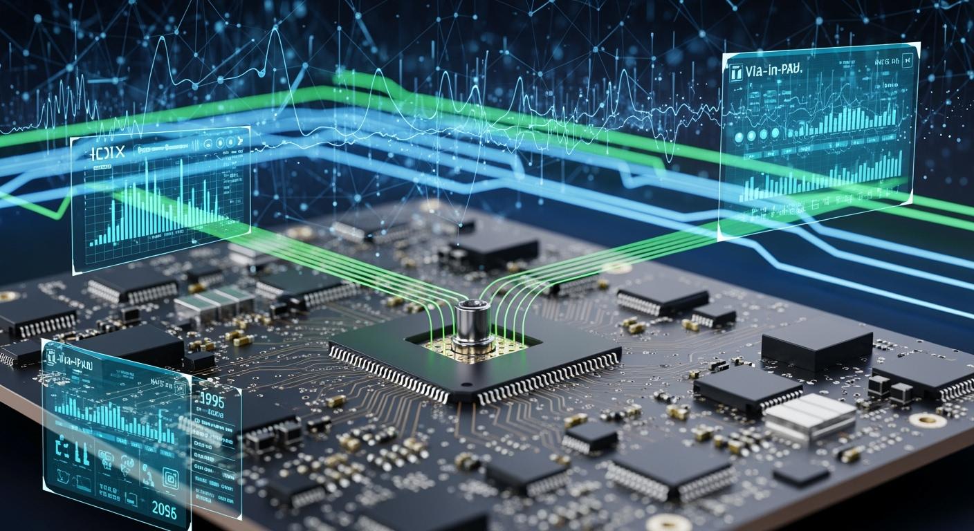
How Via-in-Pad Design Transforms HDI PCB Performance
You need via-in-pad design for HDI projects with fine-pitch SMDs and BGAs. This method gives you more space for parts. It keeps signals strong and helps manage heat. Via-in-pad technology helps make electronics smaller and thinner. You can see its effects in the table below:
Benefit | Description |
|---|---|
Smaller PCB footprint | Uses less space for each part |
Thin and lightweight devices | Makes slim designs without losing strength |
Higher component density | Lets you put parts right over vias for better space use |
You use via-in-pad design to fix hard HDI problems. It helps your products stay small and work well.
Key Takeaways
Via-in-pad design helps save space. You can put more parts on your PCB. This lets you make smaller and stronger devices.
This design makes signals travel better. The signal paths are shorter. This means less signal loss. It helps high-speed circuits work well.
Via-in-pad technology helps control heat. It moves heat away from important parts. This makes the parts last longer.
Good via filling and design make the board more reliable. Solder joints become stronger. There are fewer problems in high-density interconnects.
Working with fabricators is important. Careful checking is needed for via-in-pad design to work in HDI PCBs.
Impact of Via-in-Pad Design on HDI PCB
Space Efficiency
You want to fit more parts on your pcb. Via-in-pad design helps you do this. When you use via-in-pad, you can place components like fine-pitch SMDs and BGAs closer together. This is important for pitches of 0.65mm and below. You do not need extra space for routing traces around the pads. Instead, you can route signals right through the pad. This makes your pcb design much more compact. You can see these benefits in high-density interconnect layouts, where every millimeter counts.
You increase component density.
You simplify routing for high-density designs.
You improve thermal management, which is important for fine-pitch SMDs and BGAs.
When you use via-in-pad, you make the most of your pcb space. This is key for modern electronics that need to be small and powerful.
Signal Integrity
Signal integrity matters a lot in hdi pcb design, especially for high-speed circuits. Via-in-pad design gives you shorter signal paths. This means signals travel faster and lose less strength. You also reduce parasitic inductance by up to 50%. This helps your pcb work better at frequencies above 2 GHz. When you match impedance well, you lower signal reflections. This keeps your signals clean and strong.
Shorter signal paths reduce signal loss and crosstalk.
Lower parasitic inductance improves electrical performance.
Better impedance matching means fewer reflections and less noise.
You also get enhanced routing efficiency. Ground planes and stitching vias help keep a steady reference for signals. This is important for high-speed designs. When you use via-in-pad, you meet the tough requirements for signal integrity in modern pcb design.
Thermal Management
Heat can damage your pcb if you do not manage it well. Via-in-pad technology lets you put vias right under hot components. This gives heat a direct path to move away from the part. You can lower the temperature of key components by 5-10°C. This helps your parts last longer and work better.
In multi-layer hdi boards, you can place vias to form thermal paths. This spreads heat across the pcb. You avoid hot spots that can cause failures. In high-power applications like LED lighting and power electronics, via-in-pad design is very important. You also see these benefits in high-speed RF modules and processors.
Tip: Use filled vias in your via-in-pad design to move heat into inner copper planes. This spreads heat and keeps your pcb cool.
Reliability
You want your pcb to last a long time. Reliability improves when you use via-in-pad design. Proper via filling and good design choices help your pcb survive thermal cycling and mechanical stress. Filled vias stop solder from wicking away and prevent voids. This keeps solder joints strong.
When you follow standards like IPC-6012E and IPC-A-600K, you make sure your vias are filled and flat. This helps your solder joints stay reliable. In fine-pitch BGA packages, voids in solder joints can cause problems. Large voids increase current density and create stress points. These can lead to cracks when the pcb heats and cools. Via-in-pad design is key for routing in high pin-count BGAs, but you must manage outgassing to prevent voids.
You get better reliability in your pcb design when you use via-in-pad and follow best practices in the manufacturing process.
What Is Via-in-Pad Technology
Via-in-Pad Structure
You use via in pad to make your pcb work better. Via-in-pad puts the via right inside the pad. This lets you connect to inner layers without extra lines. You see this in hdi pcb designs where space is tight. The via in pad makes traces shorter and helps signals stay strong. It also helps heat move away from parts. This gives you better electrical and thermal results.
Tip: You can fill and cover the via in pad to make it flat. This helps with soldering and keeps your pcb easy to make.
Application in Fine-Pitch SMDs and BGAs
You need via in pad for fine-pitch SMDs and BGAs. These parts have pins very close together, often less than 0.65mm apart. You cannot use normal vias because they take up too much room. Via-in-pad lets you put vias right under the pad. You connect to inner layers without extra lines. This is important for small devices like smartphones and medical tools.
You use via in pad when you do not have much space.
You help signals stay strong for fast circuits above 500 MHz.
You make pcb design easier for BGAs and QFNs with close pins.
Via-in-pad lets you fit 20-30% more parts on your board. You can put parts closer and make the pcb smaller. You also make routing and heat control better.
Comparison with Traditional Vias
You see big changes between via in pad and normal vias. Via-in-pad sits inside the pad, but normal vias sit outside. Via in pad uses less space. It helps signals and heat move better. Normal vias cost less and are easier to make, but they need more space and longer lines.
Aspect | Via-in-Pad Design | Traditional Via Design |
|---|---|---|
Location of Vias | Inside the component pad | Outside the component pad |
Space Requirements | More efficient use of space | Consumes more space |
Manufacturing Processes | Requires precision and additional stability for HDI | Generally simpler and cost-effective |
Impact on Signal Integrity | Enhances signal integrity and thermal performance | May increase parasitic effects due to longer traces |
You pick via in pad when you want small boards and high performance. You use normal vias when you want simple boards and lower cost. Via-in-pad works best for hdi pcb, but you must follow careful steps to make it right.
Performance Enhancements with Via-in-Pad
Space Savings in HDI Layouts
Via-in-pad helps make your pcb smaller. You can put parts closer together. Signals go right through the pad, so you save space. This design can shrink your board by 30–40%. If you use fine-pitch BGA parts with a 0.4mm pitch or less, you can make the board even smaller, up to 45%. Saving space lets you add more features to your hdi pcb.
You fit more parts on the board.
You can build high-density boards.
Signal Integrity for High-Speed Circuits
You want your signals to stay strong. Via-in-pad helps keep signal integrity high. You match the via impedance to the trace, usually about 50 ohms. Back-drilling takes away unused via stubs. This stops signals from bouncing back. You also pick the right pad size to avoid extra capacitance. These steps help your signals stay clear and fast.
Note: Shorter paths and matched impedance keep signals strong.
Thermal Dissipation
Heat can hurt your pcb. Via-in-pad gives heat a way out from hot parts. You put vias under parts to move heat into copper layers. This cools your pcb and makes it last longer. You get better heat control in hdi pcb with high-power parts. You also stop hot spots that can break your board.
Connectivity in Multi-Layer Designs
You need good links in multi-layer pcbs. Via-in-pad lets you connect layers without extra lines. You use via in pad to send signals and power between layers. This makes your pcb easier to design and more reliable. You get better performance in high-density boards. You also make building the pcb easier by using fewer lines.
Tip: Use filled via in pad for strong links and better reliability.
Technical Mechanisms of Via-in-Pad
Blind Vias and Microvias
Blind vias and microvias help make your pcb better. Microvias go right under the pad, so you save space. You do not need extra pads on the back of the board. This lets you fit more parts on your hdi pcb. Microvias also help signals stay strong by lowering inductance. You use microvias in via in pad for fine-pitch BGAs, QFNs, or flip-chip parts. This makes the paths between parts shorter and helps electricity move better. You fill microvias with epoxy and cover them with metal to make them flat. This stops solder from moving away and keeps out empty spots during making. Your pcb becomes stronger and easier to put together.
Microvias help save space on the pcb.
They keep signals strong by lowering inductance.
They help heat move away through copper inside the board.
Tip: Always fill and cover microvias in via in pad to keep your pcb flat and easy to solder.
Routing Simplification
Via in pad makes routing easier in your pcb. You do not have to draw lines around outside vias. You put the via right in the pad instead. This makes your hdi pcb design simpler and can use fewer layers. You spend less money and make the pcb faster. Your high-density layout works better too. You can put vias under hot parts to help heat move through the board. This cools down important parts by 5-10°C. Your pcb lasts longer and works better.
You make trace paths simpler in your pcb.
You use fewer layers in your hdi pcb.
You help heat leave the board with via in pad.
Note: Routing is easier and quicker when you use via-in-pad in your pcb.
Layer Stackup Optimization
Via in pad helps you build your pcb layers better. You can stack or move microvias to connect layers without making the board thick. This makes the connections shorter and helps signals move faster. Via in pad also gives heat a straight path out, so your hdi pcb stays cool. Your parts work at lower temperatures and your pcb is more dependable. You can also make your board thinner, which is good for slim devices. Your pcb works better and is easier to make.
You stack microvias in via in pad for good layer links.
You make your pcb thinner.
You help signals and heat move better in your hdi pcb.
Tip: Stack microvias in via in pad to link layers and keep your pcb thin.
Challenges and Trade-Offs
Manufacturing Complexity
You face several challenges when you use via in pad in your pcb design. The manufacturing process becomes more complex. You must control every step to avoid problems. Sometimes, unfilled vias can trap moisture or dirt. This can cause corrosion or even electrical shorts in your pcb. You may also see assembly problems. If you do not align components well over via in pad, you can get poor contact or open circuits. This is a big issue for fine-pitch parts in hdi boards. Signal integrity can suffer if you do not manage parasitic capacitance and inductance. High-speed signals above 1 GHz are very sensitive to these effects. Mechanical stress is another concern. The difference in how the via and the board expand with heat can cause cracks or delamination. You must watch for these risks, especially in high-density interconnect designs.
Unfilled vias can trap moisture or dirt.
Misalignment can cause open circuits.
Parasitic effects can hurt signal integrity.
Heat can cause cracks in your pcb.
Cost Considerations
You need to think about cost when you choose via in pad for your pcb. This technology often costs more than traditional methods. The extra steps in pcb manufacturing, like filling and plating vias, add to the price. You also need special tools and skilled workers. If you want improved performance in your hdi pcb, you may decide the extra cost is worth it. You must balance your budget with your need for high-speed circuits and reliability. Sometimes, you can save money by using via in pad only in the most critical areas of your pcb design.
Tip: Use via in pad where you need the most signal integrity and space savings.
Solder Pad Integrity
You must protect the solder pads in your pcb design. Good solder pad integrity keeps your pcb reliable. You should keep the via size between 0.2mm and 0.3mm. Make the pad at least 0.1mm to 0.15mm bigger than the via on all sides. Fill or plug the via to stop solder from flowing away during assembly. Use a solder mask over the via in pad to reduce solder wicking. Place vias under fine-pitch parts in a balanced way. This helps you get even soldering and strong joints. These steps help you keep signal integrity and reliability high in your hdi pcb.
Choose the right via and pad size.
Fill vias to stop solder loss.
Use solder mask for better results.
Place vias evenly under fine-pitch parts.
You get better pcb design and improved performance when you follow these best practices for via-in-pad technology.
Best Practices for Via-in-Pad Design
Design Guidelines
You start your pcb design by planning the via in pad placement. You choose the right pad size for each component. You keep the via diameter between 0.2mm and 0.3mm. You make the pad at least 0.1mm bigger than the via. You fill the via in pad to stop solder from leaking. You use a solder mask to protect the pad. You place the via in pad under fine-pitch parts for better space use. You check the layout for high-density interconnect needs. You follow standards for pcb manufacturing. You review the design to avoid mistakes.
Tip: You use filled via in pad for strong solder joints and reliable pcb performance.
Collaboration with Fabricators
You talk to your fabricator early in the pcb design process. You share your via in pad plans and ask for feedback. You learn about their manufacturing process and limits. You ask about the best way to fill and plate the via in pad. You check if they can handle fine-pitch parts and high-density layouts. You work together to solve problems before production starts. You update your pcb design if needed. You keep clear communication to avoid delays.
Step | Action You Take |
|---|---|
Share Design Files | Send via in pad layout to fabricator |
Ask Questions | Learn about pcb manufacturing limits |
Review Feedback | Adjust pcb design as needed |
Inspection and Testing
You inspect the pcb after manufacturing. You check each via in pad for flatness and filling. You use X-ray or optical tools to find voids or defects. You test solder joints for strength. You measure signal paths to confirm performance. You look for problems with heat flow. You follow quality standards for pcb manufacturing. You fix any issues before assembly. You keep records for future pcb design projects.
Note: Careful inspection and testing help you build reliable pcb with via in pad.
Via-in-pad design changes how you build HDI PCBs. You get more space, better signals, and improved heat control. Many industries now use this method to make smaller, stronger boards. You can see the main trends below:
Key Trend | Description |
|---|---|
Technological Innovation | New HDI methods, like via-in-pad, keep improving PCB design. |
Increased Integration | Boards hold more parts and work better. |
Expanding Application Areas | More devices use HDI PCBs, from phones to medical tools. |
Cost Reduction | New drilling and microvia steps help lower costs. |
Quality Improvement | Boards last longer and work in more places. |
You should weigh the benefits and challenges. Try via-in-pad in your next HDI PCB project to boost performance.
FAQ
What is via-in-pad in HDI PCB design?
You place a via directly inside a component pad. This method helps you save space and improve signal flow. It works well for high-density layouts and fine-pitch parts.
Why should you use via-in-pad for BGAs?
You use via-in-pad for BGAs because it lets you route signals from tight pin grids. This design helps you fit more connections in a small area and keeps your board compact.
How does via-in-pad help with heat management?
You use via-in-pad to move heat away from hot parts. The via gives heat a direct path into the inner copper layers. This keeps your components cooler and helps your board last longer.
Can you use via-in-pad on any printed circuit board?
You can use via-in-pad on many boards, but it works best for high-density or advanced designs. Standard boards may not need this method. Always check with your fabricator before you decide.
What are the main risks of via-in-pad?
You may face higher costs and more complex manufacturing steps. If you do not fill the via well, you can get weak solder joints or defects. Careful design and inspection help you avoid these problems.
See Also
Evaluating Advanced HDI PCB Technologies for Future Electronics
Essential Design Factors for Reliable HDI PCB Manufacturing
The Design and Production Process of HDI Any Layer PCBs