Via-in-Pad Design for HDI PCB

You use via-in-pad design when you need more connections in a small space during pcb design. This method puts vias right under component pads. It helps you save space and use fine-pitch parts. Via-in-pad design helps your pcb by making signal paths shorter and spreading heat better. This improves signal integrity and thermal management. You may face problems like solder wicking, higher costs, and more complex designs. Careful planning and good tools can help you fix these problems. You use via-in-pad design to make strong and high-performing pcb designs for new electronics.
Common challenges and solutions in via-in-pad design:
Solder wicking: Ask for via filling and check manufacturer rules.
Increased manufacturing cost: Use via-in-pad design only where needed.
Design complexity: Use pcb design software that supports via-in-pad.
Key Takeaways
Via-in-pad design helps save space on PCBs. It puts vias right under component pads. This lets you make more connections in small spaces.
This design makes signals better by making paths shorter. It lowers inductance and cuts down on crosstalk. These things are very important for fast circuits.
Via-in-pad also helps control heat well. It moves heat away from parts, so the PCB stays cooler. This makes the board work better and last longer.
There are some problems like solder wicking and higher costs. You can fix these by using filled vias and planning carefully when you design.
If you follow rules like IPC-4761, your via-in-pad designs will work well. This keeps advanced electronics strong and reliable.
Via-in-Pad Design Overview
What Is Via-in-Pad Design
Via-in-pad design puts a via right inside a component pad on the PCB. This way is important for making high-density interconnect PCBs where space is tight, and parts are very close. By placing the via inside the pad, you save important board space. It also helps electrical signals move better. This design uses filled plated microvias, which are often smaller than 6 mils. These let you connect component leads straight to inside layers of the PCB. This makes your PCB layout more dense. It lets you fit more parts and connections in a small space without losing performance.
Note: Putting vias directly in pads is crucial for new electronics where every millimeter matters.
Why Use Via-in-Pad in HDI PCBs
You should use via-in-pad to solve space problems on PCBs with fine-pitch parts like BGAs and QFNs. This method removes the need for extra routing traces between pads by stacking vias vertically under parts.
Big benefits are:
Saves space so you can use the PCB area better.
Boosts signal quality by making paths shorter and cutting down inductance and crosstalk.
Helps manage heat because vias act as heat bridges, spreading heat away from hot parts well.
Lets you make tricky fanouts under fine-pitch arrays without losing design quality or space.
Using via-in-pad lets you make smaller, denser designs that work well for today’s tiny circuits and advanced packages.
Comparison with Traditional Vias
Here is a table showing the difference between via-in-pad and traditional vias. This helps you see how they work and how they are made:
Aspect | Traditional Via | Via in Pad |
|---|---|---|
Layout | Placed between pads or in empty areas | Built right inside the component’s solder pad |
Signal Path | Longer paths cause more inductance and signal loss | Shorter paths improve signals and reduce loss |
Space Efficiency | Needs more space because vias are separate | Saves space, allowing more parts to fit closer |
Thermal Management | Not as good at moving heat | Works as a heat bridge, moving heat away from parts |
Manufacturing | Easier to make, less filling and alignment needed | Needs via filling and pad layers, making it more complex and costly |
Choosing via-in-pad lets you create denser, better-performing PCBs but also needs more careful making and costs more. Knowing these pros and cons helps you plan your design the best way for your project.
Types of Vias in HDI
Through-Hole and Microvias
You will see two main types of vias in HDI PCB design: through-hole and microvia. Through-hole vias go from the top layer to the bottom layer of the board. They pass through every layer in a multilayer pcb. These vias are bigger and take up more space. You use them when you need strong connections across all layers.
Microvias are much smaller. You create a microvia with a laser, which gives you high accuracy. Microvias usually have a diameter between 50 and 150 micrometers. You use microvias when you want to save space and improve electrical performance. Microvias connect only the layers you need, not the whole stack. This makes them perfect for multilayer designs where space is tight. Microvias also help you control signal loss and keep your board reliable.
Microvias can be:
Blind microvias: connect the surface to an inner layer.
Buried microvias: connect only inner layers, not visible from the outside.
Stacked microvias: connect several inner layers together.
Blind, Buried, and Via in Pad
You will use different via types in a multilayer pcb. Each type has a special job. Here is a table to help you see the differences:
Via Type | Description |
|---|---|
Blind Via | Connects an outer layer to an inner layer but does not go through the entire board. |
Buried Via | Connects only internal layers and is not visible on the outer surfaces of the PCB. |
Places the via directly under the component pad, saving space and reducing trace length. |
Blind vias help you free up space on the surface. Buried vias keep connections hidden inside the multilayer pcb. The via in pad method puts the via right under the component pad. You use via-in-pad to make your design smaller and to shorten signal paths. This is very important for high-density and high-speed circuits. You will see via-in-pad used a lot in advanced multilayer pcb designs.
Applications for Fine-Pitch Components
You need via in pad and via-in-pad when you work with fine-pitch components like BGAs and QFNs. These parts have very small pads, sometimes only 0.5 mm apart. Traditional routing does not work well here. Via in pad lets you send signals straight from the pad to the inner layers. This makes your layout more compact and reduces routing problems.
Via-in-pad helps you:
Use fine-pitch parts in small spaces.
Make direct connections under the component.
Reduce the number of external vias.
Improve signal integrity by making paths shorter.
Save time and lower the chance of mistakes in your design.
You will find via in pad and via-in-pad in almost every modern multilayer pcb. They let you build smaller, faster, and more reliable boards. Microvia and microvias also play a big role in these designs. You can use them together with via in pad to get the best results for your high-density projects.
Performance Benefits of Via-in-Pad
Signal Integrity
You want your PCB to send signals that stay strong. Via-in-pad design helps you do this. When you put a via in pad, the signal path gets shorter. This means less signal loss and less crosstalk. You also lower parasitic inductance, so the board works better. Signals move fast and stay clean. You get good impedance matching, so there is less noise and fewer reflections. This matters for high-speed circuits. Active pad pcb design lets you connect signals right from the pad to inside layers. You do not need long traces or extra vias. BGA routing with via-in-pad makes it easier to route signals for BGAs and QFNs. Your signals stay strong and reliable. You can use via-in-pad anywhere signal integrity is important.
Tip: Try via-in-pad for fine-pitch parts and fast circuits. You will see better signals and less noise.
Thermal Management
You need your PCB to stay cool, especially with many parts close together. Via-in-pad helps you move heat away from hot parts. When you use via in pad, heat travels directly from the pad. Filled vias, like copper, make cooling better. You can lower junction temperature by up to 10°C compared to unfilled vias. This keeps your board safe and reliable. You can use more than one via under a pad to make a via array. This gives more paths for heat and spreads it faster. Via-in-pad cools better than traditional vias. Active pad pcb design puts vias right under the pad, so heat moves quickly to inside layers. You can use via-in-pad for power parts, LED lights, and other hot spots. Your board stays cooler and parts last longer.
Via-in-pad helps thermal management by:
Lowering junction temperature by up to 10°C.
Using via arrays to spread heat.
Giving direct heat paths through filled vias.
Copper filling makes cooling work better.
Note: Via-in-pad is important for layouts with lots of parts. It protects sensitive parts and makes your board more reliable.
High-Speed and High-Power Applications
You build PCBs for advanced electronics. You need strong performance for fast and powerful parts. Via-in-pad gives you many benefits. You can make denser PCBs and use fine-pitch BGAs. Via in pad lets you save space and fit more parts. You get better heat dissipation, which is important for power electronics. The surface stays flat, so you attach parts easily. You lower inductance and remove dog-bone pads, which helps signal integrity. You can handle higher voltage applications with confidence. BGA routing with via-in-pad supports BGAs and QFNs with high density. You make the path for signals simpler and lower inductance. Active pad pcb design lets you connect power and signal lines right under the pad. Your circuits work reliably even when they need a lot of power.
Advantage | Description |
|---|---|
Higher density PCBs | Saves space and lets you use fine pitch BGAs. |
Improved thermal dissipation | Helps manage heat, which is important for high-power parts. |
Flat and coplanar surface | Makes it easier to attach and keep parts stable. |
Lower inductance | Gets rid of dog-bone pads, so signals are better. |
Increased voltage capability | Works well for higher voltage circuits. |
Via-in-pad helps thermal management in PCB designs.
It is great for high power parts like LED lights and power electronics.
Makes signal paths simpler.
Lowers inductance, which keeps signals strong in fast circuits.
Block Quote: Use via-in-pad for fast and powerful circuits. You get better signal paths, improved cooling, and reliable performance for BGAs, QFNs, and flip-chip.
You can use via in pad and via-in-pad for active pad pcb design and bga routing with via-in-pad. You get the best results for high-density BGAs and other fine-pitch parts. Via-in-pad helps your PCB stay cool and keeps signals strong for modern electronics.
Via-in-Pad Fabrication and Challenges
Manufacturing Process
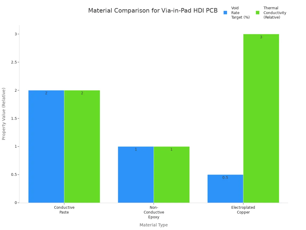
When you use via in pad in pcb fabrication, you must be careful. First, you drill small holes in the board. This makes sure the via in pad goes in the right spot. Next, you fill these holes using special materials. You can pick conductive paste, non-conductive epoxy, or electroplated copper. Filling the holes stops problems during soldering. It also keeps the electrical path strong. After filling, you add a thin metal layer around the via in pad. This is called pad metallization. It makes the connection stronger and helps signals move better. The last step is plating over or capping the via in pad. This makes the surface flat so you can put parts on top.
Material Type | Void Rate Target | Thermal Conductivity | Relative Cost | Reflow Compatibility (260°C) | Best Use Cases |
|---|---|---|---|---|---|
Conductive Paste | <2% | Moderate | Low | Good | Cost-sensitive consumer electronics |
Non-Conductive Epoxy | <1% | Low | Medium | Excellent | Standard via in pad, planarity-critical BGAs |
Electroplated Copper | <0.5% | High | Higher | Superior | High-reliability, stacked vias, thermal pads |
Common Issues and Solutions
You can run into problems when making pcb with via in pad. If you do not fill the vias, water or dirt can get inside. You should tell your manufacturer to fill or plug the vias. If things are not lined up right, the contact will be bad. You need to follow DFM rules and pick the right via size. If heat is not handled well, solder joints can get cold. You can add thermal relief patterns around the via in pad. Vias can move heat away from pads. You should use pcb software to check for hot or cold spots. For high-power parts, only use via in pad if you have no other choice.
Manufacturing Issue | Recommended Solution |
|---|---|
Unfilled vias trapping contaminants or moisture | Specify filled or plugged vias with your manufacturer. |
Misalignment of components over via in pad | Use DFM guidelines for via and pad sizes. |
Thermal issues leading to cold solder joints | Add thermal relief patterns around via in pad. |
Vias conducting heat away from pads | Simulate thermal mass in pcb fabrication software. |
Vias on pads for high-power components | Use via in pad only when space is limited. |
Cost and Reliability Factors
The process with via in pad technology is harder to do. If you do not fill the vias, water can get in and cause rust or shorts. If things are not lined up, you can get open circuits. Signals may not work well, especially if they are very fast, like above 1 GHz.
You will pay more to make pcb with via in pad. You need extra steps like filling, flattening, and capping the vias. These steps can make the board cost 15-30% more. Microvias in high density multilayer pcb can break if they are too tall and skinny. You should keep the ratio at 0.75:1 and use strong materials. Capped via in pad and plated over via in pad help keep the surface flat and strong. Even though it costs more, via in pad lets you make smaller and better boards. You get more parts and better performance, which is great for advanced electronics.
Via in pad costs more because the process is harder.
You need special materials and steps to stop soldering problems.
You get smaller and better boards for high-end devices.
Reliability and Compliance
Industry Standards
You need to follow industry standards to make sure your via-in-pad designs work well and last long. The IPC-4761 standard gives you clear rules for protecting vias. Type VII from this standard covers filled and capped vias, which help prevent solder wicking and keep your connections strong. Many manufacturers use IPC-6012 and IPC-2226 for HDI PCBs. These standards set the rules for quality, reliability, and testing. When you follow these guidelines, you make your boards safer and more reliable for high-speed and high-power uses.
Tip: Always check with your PCB manufacturer to confirm which standards they follow for via-in-pad processes.
Best Practices for Via-in-Pad
You can improve your HDI PCB design by following best practices used by industry leaders:
Place thermal vias under high-power parts to help move heat away quickly.
Use filled and capped vias to stop solder from flowing into the holes and to keep connections strong.
Follow IPC-4761 Type VII for via protection. This keeps your board safe and reliable.
Arrange vias to lower inductance and improve signal quality, especially in fast circuits.
In QFN packages, the exposed thermal pad acts as a main path for heat. If you connect this pad to a large ground plane using a group of thermal vias, you can move heat away much faster. This setup helps your board stay cool and work better.
Inspection and Testing
You must check your via-in-pad designs to make sure they are safe and reliable. Many inspection and testing methods help you find problems early:
Method | Description |
|---|---|
Advanced soldering technologies | Make strong solder joints and avoid cold or extra solder. |
Automated X-ray inspection | Find hidden solder problems and make sure vias are filled right. |
Thermal cycling | Test how vias handle changes in temperature, like in real use. |
Interconnect stress testing | Check how long vias last under stress. |
Microsection analysis | Look at plating and fill quality to make sure vias are solid. |
C-scan acoustic microscopy | Find any layers that have come apart after soldering. |
You can also use X-ray and 3D CT scans to find tiny voids, and vibration tests for tough uses like cars or planes. These steps help you catch issues before your board goes into real products.
Design Recommendations
Layout Tips
You can make your HDI PCB work better by using some easy layout tips. Always fill and cover microvias in via-in-pad. This keeps the board flat and makes soldering simple. Put parts that work together close to each other. This helps stop noise and makes signals better. Place parts so signals move in a straight line. Shorter traces help your board work faster. Spread out hot parts on the board. Use thermal vias to move heat away from these spots.
Here are some steps you can use for even better results: Place parts so machines can put them on the board easily. Leave at least 0.3 mm between parts for good soldering. Use filled vias to stop solder from leaking into holes and to make strong joints.
Tip: Smart layout choices help you avoid problems when building your board and make it last longer.
Material Choices
You need to choose the right materials for your via-in-pad design. The fill material you pick can change how well your board cools down and supports parts.
Using conductive fills like copper paste helps move heat away from parts. For example, if you use a high-power QFN, a conductive fill can lower the temperature by up to 10°C compared to non-conductive fills.
Non-conductive resin fills and copper caps give strong support but do not make an electrical connection. This is good for signal pins that do not need to connect between layers.
Working with PCB Manufacturers
When you work with a PCB maker, you need to think about some important things. Make sure the via size fits inside the pad and does not make the solder joint weak. The pad should be big enough for both the via and the solder, with enough space to stop solder bridges. Always fill or cap vias in pads to stop solder from moving into the holes. Use via-in-pad only on the top or bottom layers for surface-mount parts. Talk to your manufacturer about their process and what sizes they can make for via-in-pad.
Factor | Description |
|---|---|
Number of laminations | More laminations make the board cost more and harder to build. |
Laser drilling | Laser drilling is best for small, shallow vias. |
Aspect ratio | Keep aspect ratio low (about 0.75:1) for strong plating and good heat flow. |
Drill-to-copper clearance | Use 7–8 mils clearance for a reliable board. |
Surface finish | ENIG or ENEPIG finishes are best for high-density boards. |
Note: Always check what your manufacturer can do before you start your design. This helps you avoid mistakes and makes sure your board works as needed.
Via-in-pad design gives you lots of good things in HDI PCBs. It helps heat move away from parts faster. It also makes signal paths shorter. You can make routing easier and use fewer layers. But you may have problems like solder wicking, higher costs, and tricky manufacturing steps. You need to follow industry standards and talk with your PCB manufacturer. You should use filled vias and check your boards closely. Keep learning about advanced PCB design. Use best practices to build electronics that work well and last a long time.
FAQ
What is via-in-pad and why do you use it?
Via-in-pad puts a via right under a component pad. You use it to save space, make signal paths shorter, and help heat move away from parts. It works well for high-density designs.
Does via-in-pad increase PCB cost?
Yes, via-in-pad makes your PCB cost more. You need extra steps like filling and capping the vias. These steps help your board work better but add to the price.
How do you prevent solder wicking in via-in-pad?
You ask your manufacturer to fill and cap the vias. This stops solder from flowing into the holes. Filled vias keep your solder joints strong and reliable.
Can you use via-in-pad for all components?
You use via-in-pad mostly for fine-pitch parts like BGAs and QFNs. It helps with tight spaces. You should not use it everywhere because it costs more and needs careful planning.
What standards should you follow for via-in-pad?
You follow IPC-4761 Type VII for filled and capped vias. You also check IPC-6012 and IPC-2226 for HDI PCB rules. These standards help your board stay safe and reliable.
See Also
Essential Design Factors for Reliable HDI PCB Manufacturing
The Design and Production Process of HDI Any Layer PCBs
Advantages of LDI Exposure Machines in HDI PCB Production
