Top 10 PCB Trace Width Design Mistakes and How to Fix Them

You should make pcb trace width right. This helps your circuit stay safe and work well. Some mistakes, like overheating or voltage drops, can break traces. They can also make signals unstable. Look at the table below for easy tips:
Mistake Type | Impact on Reliability | Troubleshooting Tip |
|---|---|---|
Overheating | Can break the trace | Check voltage across the trace |
Voltage Drops | Makes circuit unstable | Make power traces bigger for real current |
Use calculators and follow industry rules for good pcbs. Try not to make pcb design mistakes. Build a strong layout for your circuit.
Key Takeaways
Always figure out the trace width for the current load. This stops overheating and keeps your PCB working well.
Use trace width calculators to find the right width. This helps you avoid guessing in your PCB design.
Check manufacturing tolerances so your design meets standards. This also helps you avoid losing signals.
Think about heat effects when you design. Keep trace temperatures safe to make sure your PCB works well.
Keep enough space between traces to stop electrical shorts. This also keeps your signals strong and clear.
Common PCB Trace Width Mistakes
Underestimating Current Load
Some people think thin traces are fine for any circuit. This is a mistake many make with pcb trace width. If a trace is too thin for the current, it can get too hot. The trace might even break. Many surveys show these problems happen a lot:
Traces are too thin for the current they need to carry
Not enough space can cause arcing or signal problems
High-speed differential pairs can have uneven impedance
Some people ignore the smallest spacing the manufacturer allows
If you guess wrong about the current, bad things can happen. You might see delamination, parameter drift, or connector arcing. Check this table to see how too much current can hurt your pcb:
Mechanism | Threshold Current | Failure Mode | Typical Impact Time |
|---|---|---|---|
Trace Overheating | >3A/mm² width | Delamination | Hours to days |
Component Stress | >80% of I(max) | Parameter drift | Weeks to months |
Connector Arcing | >20A per pin | Contact corrosion | Immediate to weeks |
Here is a real example. A medical device stopped working after 200 hours. It used a 0.75mm trace that carried 2.3A. The trace should have been at least 1.2mm wide, based on IPC-2152 rules. Always check the current for each trace to stop these problems.
Not Using Trace Width Calculators
You should not guess the width of your traces. A trace width calculator helps you follow the rules and keeps your design safe. Here are the steps you should take:
Find out how much current the trace can carry with its copper thickness.
Set a limit for how much the trace can heat up.
Use a trace width calculator to get the smallest width you need.
Change the numbers if you need to meet your design goals.
Make sure the trace width works with how the board is made.
Tip: Online calculators from Advanced Circuits or Saturn PCB Design make this easy. PCB design software like Altium Designer, KiCad, and Autodesk Eagle also have tools for this. These calculators are usually right within 5-10%. Some advanced tools are even more exact.
A trace width calculator helps you follow IPC-2221 or IPC-2152 rules. You also avoid common pcb design mistakes and make your pcb stronger. Good calculators show how current, heat, and trace width work together. This keeps your signals strong and your board safe.
Incorrect Trace Width and Spacing
Overlooking Manufacturing Tolerances
You need to watch manufacturing tolerances when you design a pcb. These tolerances show how much the trace width can change in production. Most factories let the width change by about ±10% to ±20%. If you do not check these numbers, you may have big problems. Small changes in trace width and spacing can cause signal loss. They can even make your pcb stop working.
Here are some common problems from wrong trace width and spacing:
Inner layer over-etching can make traces very thin.
Less copper thickness lowers how much current the trace can carry.
Lower electrical reliability can make your circuit fail.
Minimum trace width and spacing are needed for good etching and plating. If traces are too narrow or too close, you can get shorts or opens. Always follow spacing rules to keep your pcb safe and reliable.
Fixing Layout Errors
You can stop many pcb layout errors by checking your design before sending it to the factory. Start by looking at the target impedance and how your transmission lines are built. Make sure you think about the thickness of the dielectric and where the ground copper is. This helps you choose the right trace width for your signal.
Remember these tips to fix layout errors:
Keep proper ground clearance and return path continuity.
Do not use the same trace width on different layers.
Watch for nearby copper that can affect your trace.
Use reference tables to check the minimum spacing for your pcb. Here is a quick guide based on IPC standards:
Standard | Class 1 & 2 (Low Voltage) | Class 3 (Low Voltage) | High Voltage (Class 2 & 3) | Additional Notes |
|---|---|---|---|---|
IPC-2221 | 0.25mm (10 mil) | 0.15mm (6 mil) | 0.5mm (20 mil) | Guidelines for different classes of PCBs |
IPC-2222 | 0.25mm (10 mil) | 0.15mm (6 mil) | N/A | Based on voltage levels |
UL 796 | 0.8mm (32 mil) | N/A | 1.6mm (64 mil) | For low-voltage conductors |
J-STD-001 | 0.25mm (10 mil) | 0.18mm (7 mil) | N/A | Minimum spacing between pads and traces |
MIL-PRF-55110 | 0.25mm (10 mil) | 0.15mm (6 mil) | N/A | Based on insulation requirements |
IEC 60601-1 | N/A | N/A | 4mm (0.16 inch) | For power supply components |
Tip: Always check your pcb layout for trace width and spacing mistakes before production. This step helps you avoid expensive errors and keeps your design strong.
PCB Trace Width and Temperature Rise
Ignoring Heat Effects
You need to think about heat when you design a pcb. If you forget about heat, you can make big mistakes. Too much heat can hurt your trace. It can also lower how much current the trace can carry. Not planning for heat can cause these problems:
Traces get too hot
Traces carry less current
Bad heat control can make parts fail
Thermal spacing is just as important as electrical spacing. If spacing is wrong, traces can get very hot. This can break signals or make the pcb stop working. Do not guess the spacing or width for your trace. Always check the heat limits before you finish your design.
Calculating for Safe Operation
There are easy ways to keep your pcb safe from heat. The IPC-2221 rule says traces should not get hotter than 20°C above normal. Most designers use this rule to stop heat problems:
The IPC-2221 calculator sets the highest allowed temperature rise for pcb traces at ΔT = 20°C.
Thermal studies show how trace width changes the temperature rise. Look at this table to see how different widths change the trace temperature when the room is 40°C:
Temperature Rise | Trace Width | Actual Trace Temperature (40°C ambient) |
|---|---|---|
5°C | 95 mil | 45°C |
10°C | 55 mil | 50°C |
20°C | 32 mil | 60°C |
You can use different ways to find safe thermal spacing and width for your trace:
Method | Equation/Parameters | Notes |
|---|---|---|
IPC 2221 | I = kΔTbAc (k = 0.048 for visible traces, 0.024 for internal tracks) | Uses one graph and equation; works best in certain ranges. |
IPC 2152 | Uses a Universal Chart to find unadjusted cross-sectional area | More exact; uses many things to find the right area. |
General | Minimum trace width = 1.0 mm/A for 1.0 oz/ft2 copper thickness | Simple rule for trace width based on current. |
Always use the right way to check thermal spacing. This helps you stop signal loss and keeps your pcb working well. Good heat design means you pick the right trace width, spacing, and current for every part of your board.
PCB Layer Thickness Errors
Misjudging Copper Thickness
You need to check copper thickness when you design a pcb. Picking the wrong copper weight can cause problems with spacing and making the board. If you use the wrong copper, traces can fail and carry less current. Thicker copper helps with heat, but it makes building the board harder. If copper is not even, your board can bend or twist. This makes it harder to build and put together. Keeping copper thickness steady helps high-speed signals stay strong. If copper thickness changes, you can get more crosstalk and lose signals.
Here is a table that shows how copper thickness affects your pcb:
Aspect | Impact |
|---|---|
Electrical Properties | Wrong thickness can make traces fail and carry less current. |
Thermal Management | Thicker copper helps with heat but makes building harder. |
Mechanical Properties | Changes in thickness can bend or twist the board and make assembly tough. |
Impedance Control | Steady thickness is important for high-speed signal paths. |
Signal Quality | Thickness changes can hurt signal quality and cause more crosstalk. |
Thicker copper lets you carry more current without overheating. IPC-2221 charts help you pick the right trace width and copper thickness for power lines. If you double copper thickness, you can carry more current with the same trace width.
Here are standard copper weights and their thicknesses:
Copper Weight (oz/ft2) | Thickness (mils) | Thickness (μm) | Weight (g/m2) |
|---|---|---|---|
0.25 | 0.34 | 8.9 | 76 |
0.5 | 0.69 | 17.5 | 152 |
1.0 | 1.37 | 35 | 305 |
1.5 | 2.06 | 52.5 | 457 |
2.0 | 2.74 | 70 | 610 |
3.0 | 4.11 | 105 | 915 |
4.0 | 5.48 | 140 | 1220 |
5.0 | 6.85 | 175 | 1525 |
6.0 | 8.22 | 210 | 1830 |

Adjusting for Actual PCB Specs
Always match your design to the specs from your pcb manufacturer. This helps you avoid problems and keeps spacing right. First, find traces that need tight tolerances, like high-speed signals or power traces. Use your design software to set rules for trace width and spacing. Add notes in your files to show the allowed range for important traces. Before you build, ask your manufacturer if they can meet your needs.
Here are some tips to help you adjust for real pcb specs:
Design with margin. Make traces a bit wider than the minimum so they do not get too narrow during manufacturing.
Pick the right copper weight. Thicker copper, like 1 oz/ft2, helps with etching and lowers tolerance problems.
Do not use very tight tolerances unless you need them. Most manufacturers have standard limits for spacing and making boards.
If you follow these steps, you will make fewer mistakes and build boards easier. You will also keep spacing and trace width safe for every pcb you make.
Voltage Drop in PCB Traces
High Resistance Issues
You need to watch for high resistance in your pcb traces. High resistance can cause a big voltage drop, which hurts your circuit. If you do not account for voltage drop, your design can fail. Ohm's Law shows that voltage drop depends on the current and the resistance of the trace. When you use a narrow trace, resistance goes up. This makes the voltage drop higher when current flows. If you increase the width of your trace, resistance drops. This keeps the voltage steady and helps your circuit work well.
Many mistakes happen when you do not check for high resistance. Here are some common causes:
Poor pcb design can make resistance too high. You may not see this until your board is working.
Moisture can get into the board and raise resistance. This can cause high-leakage current.
Not keeping enough spacing between traces can lead to problems.
You can fix these issues by following good design rules. Always keep proper spacing and use the right materials. Make sure you use the correct pcb trace width for the current you need.
Minimizing Signal Loss
You want to keep your signal strong as it moves across the pcb. Signal loss happens when voltage drops too much. You can lower signal loss by using smart design steps:
Use wider traces for higher current. This lowers resistance and keeps voltage steady.
Keep spacing between traces wide enough to stop crosstalk.
Use smaller microvias and HDI pcb technology to cut down on discontinuities.
Route traces in a daisy chain instead of using many branches.
Add proper terminating resistors at the start and end of your signal lines.
Use differential signaling and keep pairs close together.
Make signal return paths as wide as possible, especially near connectors.
Use a solid ground plane to give signals a low-resistance path back.
Tip: Always check your layout for not accounting for voltage drop. This step helps you avoid common mistakes and keeps your pcb reliable.
If you follow these steps, you will keep your signals clear and your circuit safe. Good spacing, the right trace width, and careful design stop voltage drop from hurting your board.
Signal Integrity and PCB Trace Width
EMI and Crosstalk Problems
You must keep your circuit safe from EMI and crosstalk. These problems happen if trace spacing or width is wrong. Not thinking about signal integrity causes high-speed PCB mistakes. Using the wrong trace width can mess up impedance. This makes signals bounce back and adds noise. You might see signals get fuzzy or act strange. These issues can hurt your whole system.
Here are ways bad trace width and spacing cause trouble:
Impedance mismatches make signals weaker. This is a big problem for fast circuits.
If impedance is not steady, you get more signal bounce. This makes signals worse and weakens communication.
The biggest trace width you use affects signal strength in fast PCB designs.
Bad spacing lets signals jump between traces. This causes crosstalk and EMI.
Changes in impedance along the trace make signals bounce. This brings more signal problems.
Tip: Always check your trace spacing and width before you finish. This helps you avoid mistakes and keeps signals clear.
Optimizing for High-Speed Signals
You can stop high-speed PCB mistakes by using good design steps. Good design keeps signals strong. Start by matching impedance. Use tools or calculators to pick the right trace width for your goal. High frequencies need more care because they are easy to mess up.
Follow these steps to keep signals strong:
Match impedance for every trace. Use tools to help.
Think about frequency. Faster signals need tighter control.
Design with manufacturing limits in mind. This keeps impedance steady.
Route traces with the same width. Do not change width suddenly.
Put a solid ground plane under fast traces. This keeps spacing and impedance even.
Always check your spacing and trace width for every fast signal. This stops signal problems and keeps your PCB working well.
Generic Widths vs. Calculated PCB Trace Width
One-Size-Fits-All Pitfalls
Some people use the same trace width everywhere. This seems easy, but it causes mistakes. Every trace needs a width that fits its job. If you use one width for all traces, you can get overheating. You might also have bad spacing and weak signals. Some traces carry more current than others. Some need special spacing to stop crosstalk. If you ignore these needs, your pcb might not work.
Many designers pick generic widths to save time. This shortcut leads to problems. You could see voltage drops or broken traces. Spacing errors can cause shorts. Always check the rules for spacing for each trace. Do not let one-size-fits-all thinking hurt your design.
Note: Using the same width for all traces skips the special needs of each circuit. You should match spacing and width to what each trace does.
Customizing for Circuit Needs
You can make your pcb stronger by picking the right trace width and spacing. Start by setting minimum, preferred, and maximum widths for each trace. Use routing tools to check spacing as you build your design. Simulation tools help you see how spacing changes signal quality.
Here is a table that shows how you can pick trace width for different circuit needs:
Feature | Description |
|---|---|
Minimum Trace Width Rules | Lets you set minimum, preferred, and maximum trace widths in PCB design. |
Interactive Routing Tools | Checks if you follow design rules while routing. |
Simulation and Design Utilities | Gives tools for high-speed design and working with manufacturers. |
You can use these ways to make your pcb better:
IPC-2221 calculator helps you pick the right trace width for safe temperature rise.
Unified design models let you set trace sizes inside design rules.
You can share your project with manufacturers and check spacing before making the board.
When you pick the right trace width and spacing, you avoid common mistakes. Your pcb works better and lasts longer. You keep signal paths strong and stop shorts. Always use the right spacing for each trace. This step helps you build circuits that work well.
Environmental Factors in PCB Design
Humidity and External Conditions
You need to think about the environment when making a pcb. Humidity and temperature changes can cause problems. Water in the air can get inside your board. This can make layers come apart and stick less. Big temperature changes can crack solder joints or break your board.
Here is a table that shows how these things affect pcb trace width reliability:
Environmental Factor | Impact on Trace Width Reliability |
|---|---|
Humidity | Can lead to delamination and reduced adhesion of layers |
Temperature Fluctuations | Causes solder joint fatigue and potential catastrophic failure |
Mistakes in picking materials or not thinking about these stresses can make your board fail. You should always check how your pcb handles moisture and heat. If you do not, you might see signal loss or your board could stop working.
The thermal cycling test checks how well a PCB handles temperature stress. It switches between hot and cold many times. This test finds big problems like CTE mismatches and solder joint fatigue.
Adapting Trace Width
You can make your pcb stronger by changing trace width for tough conditions. Start by checking the board’s temperature and how much heat your design allows. This helps you pick the right width for each trace. You should also follow IPC-2221 rules to find the best width for your current and temperature rise.
Here are some ways to change your design for harsh conditions:
Use thicker copper layers to lower resistance and help with heat.
Spread current across more layers and use thermal vias for better heat control.
Add heat sinks to move heat away from high-power spots.
Always check your spacing rules. Good spacing stops moisture from causing shorts and keeps signal paths clear.
Review your spacing after every design change. This helps you avoid mistakes and keeps your board safe.
Design Modification | Description |
|---|---|
Trace Width | Designers should select appropriate trace widths to balance current capacity and thermal performance. |
Copper Thickness | Using thicker copper layers can help reduce resistance, especially in high-current applications. |
Heat Management | Effective thermal management involves spreading current load across multiple layers and using thermal vias. |
If you check your spacing and trace width for every part of your pcb, you will stop many common mistakes. Your signals will stay strong, and your board will last longer.
Overcrowding and Common PCB Design Mistakes
Insufficient Clearance
You need to keep enough spacing between traces on your pcb. If you do not, you can cause many common pcb design mistakes. When traces are too close, you risk electrical shorts and signal problems. Overcrowding happens when you try to fit too many traces or components in a small area. Incorrect component placement can make spacing even worse.
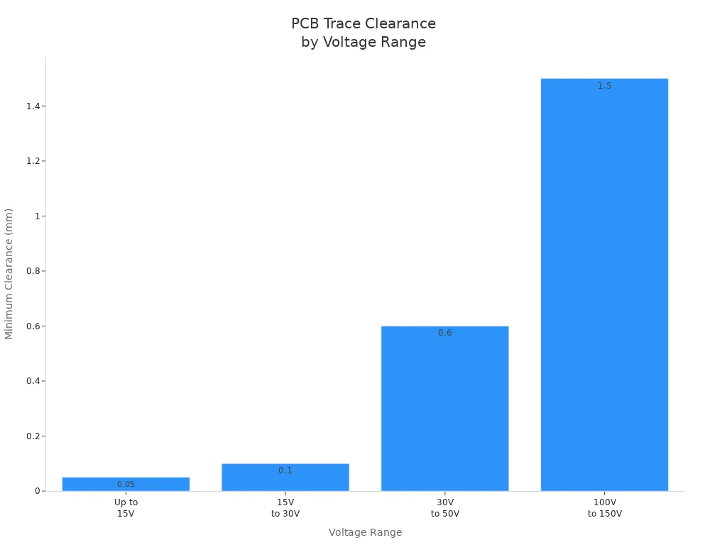
You should always check the minimum clearance for your voltage range. IPC standards give clear rules for safe spacing. Look at this table to see the recommended minimums:
Voltage Range | Minimum Clearance |
|---|---|
Up to 15V | 0.05 mm (2 mils) |
15V to 30V | 0.1 mm (4 mils) |
30V to 50V | 0.6 mm (24 mils) |
100V to 150V | 1.5 mm (59 mils) |
If you do not follow these spacing rules, you can get arcing or even fire. You also make it hard for the factory to build your board. Always plan your design so you have enough room for each trace and component.
Preventing Shorts
You can stop shorts by using good spacing and careful layout. Start by checking your pcb trace width and the space between traces. Use your design software to set rules for minimum spacing. Make sure you do not place traces under components where you cannot see them. Always keep spacing wide enough for the voltage you use.
Here are some tips to prevent mistakes:
Use wider spacing for high voltage.
Check all layers for crowded spots.
Avoid sharp corners in traces.
Review your layout for incorrect component placement.
If you follow these steps, you lower the risk of shorts and keep your pcb safe. Good spacing also helps your signal stay strong and your board last longer.
Power vs. Signal Trace Width in PCB
Differentiating Trace Types
You need to know the difference between power and signal traces when you design a pcb. Power traces carry high current. Signal traces carry information between parts. Each trace needs the right width and spacing. If you mix them up, you can make common pcb design mistakes.
Power traces need more spacing because they get hot and can cause shorts. Signal traces need careful spacing to keep signals clear. You should always check the return current path for each trace. This helps you stop noise and keeps your board safe.
Here is a table to help you see the main differences:
Trace Type | Current Level | Main Focus | Spacing Needs |
|---|---|---|---|
Power | High | Heat, safety | Wide spacing |
Signal | Low | Signal quality | Controlled spacing |
Tip: Always label your traces in your design. This helps you pick the right spacing and stops mistakes.
Sizing for Power Handling
You must size power traces for the current they carry. If you use the wrong width, the trace can overheat. This can break your pcb. Use a pcb trace width calculator to find the right size. Always check the spacing around power traces. This stops arcing and keeps your board safe.
Signal traces need less width, but you still need good spacing. This keeps the signal strong and stops crosstalk. You should keep the return current path short and wide. This lowers noise and helps your circuit work well.
Follow these steps to size your traces:
Find the current for each trace.
Use a calculator to set the right width.
Check spacing rules for your voltage.
Review your design for mistakes.
If you follow these steps, you will avoid common pcb design mistakes. Your pcb will last longer and work better.
Verification Tools for PCB Trace Width
Simulation and Double-Check
You can stop many mistakes in pcb trace width by using simulation tools. Simulation lets you see how your design will work before you build it. You can check spacing, width, and signal paths. Simulation tools show you if your traces get too hot or if spacing is too tight. You can spot problems early and fix them. Many pcb design programs have built-in simulators. These tools help you double-check your layout and spacing. You can test for signal loss and see if your trace width is safe for the current. Simulation also helps you find weak spots in your pcb. You can change spacing or width to make your board stronger.
Tip: Always run a simulation before sending your pcb to the factory. This step helps you catch mistakes and keeps your design safe.
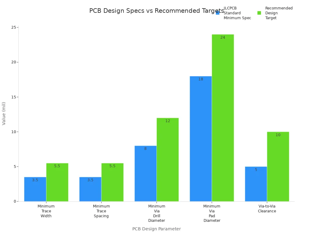
You can use tables to compare your design to factory standards. Look at the table below to see the minimum specs and recommended targets for spacing and trace width:
Parameter | JLCPCB Standard Minimum Spec (1 oz Copper) | Recommended Design Target (For Optimal Yield) |
|---|---|---|
Minimum Trace Width | 3.5 mil (0.09mm) for Multilayer | 5.0 to 6.0 mil |
Minimum Trace Spacing | 3.5 mil (0.09mm) for Multilayer | 5.0 to 6.0 mil |
Minimum Via Drill Diameter | 0.2 mm (8 mil) | 0.3 mm |
Minimum Via Pad Diameter | 0.45 mm (18 mil) | 0.6 mm |
Via-to-Via Clearance | 5.0 mil (0.127mm) for 4L+ | 10.0 mil |
Using Online Calculators
You can use an online calculator to check your pcb trace width and spacing. Calculators help you find the right width for each trace. You can enter your current, copper thickness, and spacing needs. The calculator shows you the best width for your design. You can use a calculator to check spacing between traces. Many calculators let you test for signal loss and heat. You can use a calculator to compare your design to industry standards. You can find calculators in pcb design software or on websites. You can use a calculator to check spacing for power and signal traces. You can use a calculator to test spacing for high-speed signals. You can use a calculator to check spacing for different layers. You can use a calculator to check spacing for vias and pads. You can use a calculator to check spacing for crowded areas.
Note: You can use a calculator to double-check your spacing and trace width. This step helps you avoid mistakes and keeps your pcb strong.
You can make your pcb work well if you avoid mistakes with pcb trace width. Always use calculators, tables, and simulation tools to check your design. Pick the right width and spacing for each trace. Good spacing keeps signals strong and stops issues. Review your spacing rules often. Share your spacing tips with your team. Keep learning about spacing to make your pcb designs better.
Use calculators to find trace width and spacing.
Check spacing for each trace and signal.
Follow the rules for spacing in the industry.
Watch out for mistakes and keep your pcb safe!
FAQ
What is the best way to set spacing between traces on a PCB?
You should follow IPC standards for spacing. Check your voltage and current needs. Use your design software to set rules. Always review your layout for crowded spots. Good spacing helps prevent mistakes and keeps your board safe.
How does trace width affect signal quality?
Trace width controls how much current flows and how strong your signal stays. If you use the wrong width, you can lose signal strength. Always match the width to your design needs. This step helps you avoid common mistakes.
Why do spacing mistakes cause PCB failures?
Spacing mistakes can lead to shorts, arcing, or weak signals. If traces are too close, you risk damage. You should always check spacing rules for your voltage and current. Careful design stops these problems.
How can I check if my spacing is correct?
You can use online calculators or your PCB design software. These tools help you measure spacing between traces, pads, and vias. Always compare your results to industry standards. This step helps you avoid mistakes.
Does spacing change for power and signal traces?
Yes, spacing changes based on the trace type. Power traces need wider spacing to handle heat and high current. Signal traces need controlled spacing to keep signals clear. Always set spacing rules for each trace in your design.
See Also
Addressing Common Issues in PCB Design for SMT Needs
Effective Approaches to Reduce Back Drilling Costs in HDI PCBs
Ten Strategies for Reducing Expenses in Custom PCB Manufacturing
