PCB Miniaturization Unlocks Smaller, Smarter Devices
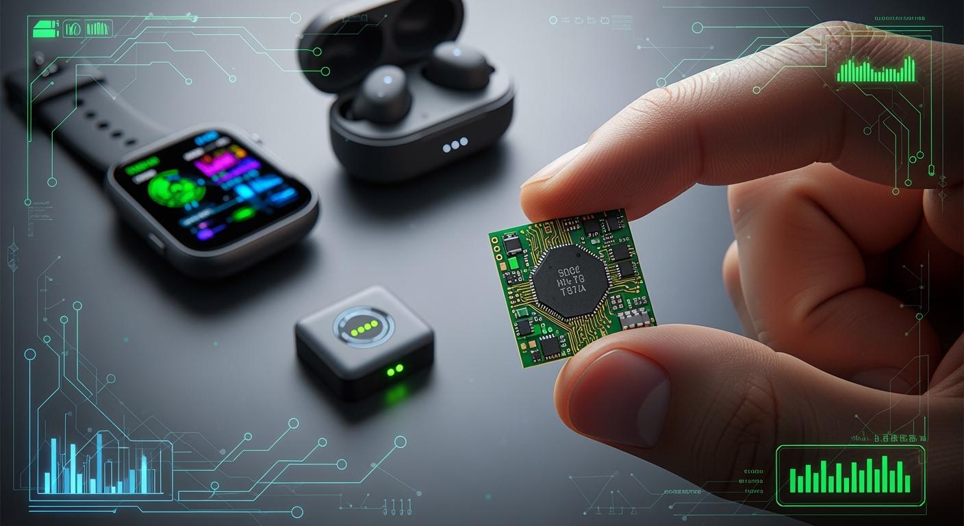
PCB miniaturization is making circuit boards smaller but just as good or better. You can use design skills to put more parts in a small space. This helps make things like smartwatches and earbuds. Today’s smartphones have over 1,000 parts on a pcb smaller than 100 cm². The market for miniaturization is growing quickly. It is expected to grow by 11.4% each year from 2026 to 2033. Think about how you can use these ideas in your own projects to make smarter devices.
Key Takeaways
PCB miniaturization helps make devices smaller but still strong. This lets you build lighter and easier-to-carry gadgets.
High-density interconnects (HDI) let you add more parts in small spaces. Use thinner lines and smaller holes to make your board work better.
Thermal management is very important in small designs. Add thermal vias and heat sinks to stop overheating and keep devices working well.
Try new design ideas like flexible and rigid-flex PCBs. These help you make cool shapes and improve how devices work.
Pay attention to quality control and exact manufacturing tolerances. This makes sure all parts fit right and signals stay strong.
What Is PCB Miniaturization?
Practical Meaning in Electronics
You may ask what pcb miniaturization means for your work. In electronics today, pcb miniaturization is making printed circuit boards smaller than usual. You do not lose any features or performance. Sometimes, you get even more. You can fit extra functions into a tiny space. This makes devices lighter and easier to carry. You see this in things like smartwatches and earbuds. Fitness trackers also use these ideas. Designers use special ways to put more power in less space.
When you do pcb miniaturization, you use high-density interconnects, called hdi. This lets you place more parts and connections close together. You also use fine-pitch parts and special assembly steps. These help keep the board dense but still high quality. You can make circuit boards that are small and strong.
Tip: Use the best design tools and materials. This helps you handle miniaturization problems and keeps your pcb working well.
Evolution of PCB Size
PCB size has changed a lot in twenty years. Now, boards are much smaller and thinner in new devices. Rigid-flex pcbs mix hard and bendable layers. This lets boards fit into tight and odd shapes. Flexible pcbs are popular because they save space. They also make devices more reliable when they move or bend.
In the early 2000s, most boards had traces and spaces about 5-6 mil. Some advanced makers got this down to 3.5 to 4.5 mil. This shows how far miniaturization has come. Smaller parts and multi-layer designs let you build complex boards in less space. You can now make products that are smarter and more efficient. They are also easier to use.
You get many benefits from these changes:
Devices are easier to carry and use less energy.
You can add more features without making things bigger.
Advanced layers and density give better performance in a small size.
Core Concepts in PCB Miniaturization Design
High-Density Interconnects (HDI)
High-density interconnects help you fit more parts and connections on your printed circuit boards. HDI uses special ways to make the board more crowded with parts. This lets you put more pieces in a small space. You get thinner lines, smaller holes, and more layers. These things help you add more features without making your pcb bigger.
Thinner lines and spaces let you add more connections in a tight spot.
Smaller holes and pads help you fit extra parts.
Blind and buried vias, plus microvias, let you pack in more connections.
Here are some HDI techniques you might use:
Technique | Description |
|---|---|
Microvia Drilling | Uses lasers to make tiny holes (0.1 mm or less) for connecting layers. |
Fine Line Etching | Makes very thin copper lines (as thin as 2 mils) to save space. |
Sequential Lamination | Builds boards in steps, so you can have many layers (6 to 20 or more). |
Tip: HDI helps you make smaller and smarter devices by letting you fit more in less space.
Layer Stack-Up & Thin Materials
You can make your pcb smaller by using special layer stack-up methods and thin materials. These ways help you arrange and space out the layers better. Thinner materials make the board less thick. You can use interlayer offset and stack-up measling to get the thickness you want and still have good performance.
Special layer stack-up methods help you spread out layers and space them well.
Thinner materials make the board less thick.
Interlayer offset and stack-up measling help you reach the right thickness.
Here are some thin materials you might use for miniaturization:
Material Type | Description |
|---|---|
Low-Dk/Df Laminates | Help stop signal loss in high-frequency uses. |
Thin Substrates | As thin as 0.1 mm, let you stack more layers for small designs. |
Conductive Inks | Print circuits on bendy materials for light, flexible boards. |
You can also use very thin rigid, flexible, or rigid-flex boards. These use thin copper, polyimide, and glue to make the board even smaller and lighter.
Fine-Pitch & Small Components
Fine-pitch and small components let you put more features on your boards. Fine-pitch means the pins on a part are very close together. This lets you place more parts in a small area. You see this in things like phones and medical tools, where space is tight.
Fine-pitch parts let you fit more circuits in less space.
This is important for small and advanced products.
Consumer electronics and medical devices use miniaturization a lot.
When you put small parts on a board, you must be careful. Each part needs to be placed just right. Heat is harder to control as parts get smaller. Tiny parts can break if you push too hard during assembly. It is also hard to check small parts because they are tiny. You need special ways to build these boards and keep them working well.
Microvias and Advanced Vias
Microvias and advanced vias help you connect layers in crowded boards. Microvias are tiny holes that link layers in your pcb. They give signals a shorter path, which helps keep signals strong. Microvias lower unwanted effects like capacitance and inductance, which is important for fast signals. They also help move heat away from busy spots.
Benefit | Description |
|---|---|
Improved Routing Density | Microvias let you put parts closer and have more ways to connect. |
Enhanced Signal Integrity | Shorter paths keep signals strong, which is good for fast signals. |
Reduced Parasitic Effects | Lower capacitance and inductance help stop problems in fast designs. |
Better Thermal Management | Microvias help heat move away from hot spots. |
Flexibility in Design | Stacked and staggered microvias let you make tricky connections between layers. |
You must make sure microvias are filled well. Filling tiny holes with metal is hard. If you do not fill them right, you can get empty spots or mistakes. These problems can make your pcb stop working. Good quality is very important, especially as microvias get smaller.
Signal Integrity & Crosstalk
Signal integrity is harder when your pcb gets smaller. When traces are close, signals can mess with each other. This is called crosstalk. You also get problems like weak signals and mismatched impedance. Fast signals in small boards make these problems worse.
You can try these ways to lower crosstalk:
Make parallel traces shorter to cut down crosstalk.
Use lower Dk materials to lower crosstalk by up to half.
Put traces close to reference planes to keep fields inside.
Leave enough space between traces.
Do not put signal layers next to each other, or run traces in different directions.
Note: Good signal integrity keeps your boards working well, even when you make them very small.
Thermal Management in Miniaturized PCBs
Thermal management is tough in small pcb designs. When you put more parts in a small space, heat builds up fast. High power density means you need better ways to move heat away from hot spots. If you do not control heat, parts can wear out, your system can have problems, or you can get thermal runaway in powerful devices.
Here are some good ways to manage heat:
Thermal vias move heat from hot parts to cooler places or heat sinks.
Built-in heat pipes use liquid to carry heat away from important spots.
Active cooling, like Peltier coolers or liquid cooling, keeps things cool even when working hard.
You need to plan for these solutions when you design your board. This keeps your printed circuit boards working well and performing great, even as you make them smaller and smarter.
Miniaturization Design Challenges & Solutions
Common Obstacles in PCB Miniaturization
When you make printed circuit boards smaller, new problems show up. Here are some common issues you might face:
Thermal management problems can make boards heat up fast and peel apart.
Thin boards can bend and twist when they cool down.
It is hard to check hidden joints, so you need special tools like X-ray.
Making sure parts are placed and lined up right is tricky.
You must watch manufacturing tolerances closely. Tight tolerances help parts fit well and keep signals strong. As boards get more crowded, you need to be exact. This makes sure connectors fit, vias land right, and traces are correct. Being precise is important for how well next-gen pcbs work.
Strategies for Next-Gen PCBs
You can solve these problems by using smart strategies. Careful planning helps your boards work better and last longer.
Plan trace lengths early to stop signal delays and reflections.
Use layer stack-ups to keep fast signals away from power and ground planes.
Make ground planes a priority to keep impedance steady and block interference.
Test your design with simulations to find problems before making the board.
Pick materials that handle fast signals and move heat well.
To get rid of heat, you can:
Use thermal relief pads on power parts.
Make sure the case has good airflow.
Add thermal vias to move heat away from hot spots.
Find and fix hot spots to stop signal problems.
Put in heat sinks to spread heat out.
Advanced simulation tools like Quanscient Allsolve help you fix miniaturization problems. These tools use cloud computing to run many tests at once. You can check different designs quickly. Domain decomposition and parallel simulations make tests faster, so you can try more ideas.
By using these best practices, you build boards that are dense and work well. You get reliable performance and keep quality in ic and part placement. Miniaturization lets you make smarter devices.
Impact of Miniaturization on Next-Gen PCBs
Smaller Form Factors
Miniaturization makes devices smaller and lighter. You can carry them more easily. This is because more parts fit on each pcb. Designers use new ways to shrink circuit boards. They do not lose any power or speed. People want tiny gadgets, so companies make thinner phones and lighter wearables. You also see this in laptops and smartwatches.
Here is how miniaturization changes electronics:
Evidence | Description |
|---|---|
Demand for Ultra-Compact Solutions | The electronics industry wants smaller packaging for all types of devices. |
Pressure on Manufacturers | Companies must make thinner, lighter, and more portable products with better features. |
Market Opportunity | New pcb technologies give you more space efficiency than old rigid-flex circuit boards. |
You can put parts closer together to save space.
Smaller boards let you add more features to things like drones.
You see tiny satellites, smart glasses, and micro UAVs because of this.
Miniaturization lets you use more layers and higher density. You can build next-gen pcbs that fit in very small spaces. This helps you meet the needs of today’s electronics.
Enhanced Device Intelligence
Miniaturization does not just make things smaller. It also makes them smarter. Small printed circuit boards let you add cool features. You do not need to make the device bigger. Microvias help connect more layers in a small area. This means you can add sensors, processors, and wireless chips.
Microvias let you fit more parts in less space.
You get better electrical performance and heat control.
You can add complex features to things like phones and medical tools.
You see smartwatches that track your health. Glasses can show you information. Drones can fly with smart controls. These devices use next-gen pcbs to be powerful and small. You get more features, better quality, and strong performance. Miniaturization changes how you design and use electronics.
You now know that pcb miniaturization helps you fit more features in small spaces. Important ideas are high-density interconnects, flexible boards, rigid-flex boards, and embedded parts. These advanced pcb methods let you make devices thinner and smarter. When you learn these design skills, you help create new things and make your projects better. Focus on learning technical skills, use the best tools for making boards, and check quality all the time. In the next five years, electronics will get even smaller and faster and change the world.
FAQ
What is the main goal of PCB miniaturization?
You want to fit more features into a smaller space. This helps you make devices lighter, smarter, and easier to carry. Miniaturization lets you add new functions without making your device bigger.
How does HDI technology help you?
HDI lets you place more parts close together. You use thinner lines and smaller holes. This makes your board smaller and more powerful.
Why do you need special tools for miniaturized PCBs?
You need special tools to check tiny parts and hidden joints. X-ray machines help you see inside the board. These tools make sure your board works well and stays reliable.
What problems can you face with small PCBs?
Heat builds up fast.
Parts can be hard to place.
Checking for mistakes is tricky.
You must plan your design and use good materials to solve these problems.
See Also
Evaluating Advanced HDI PCB Technologies for Future Electronics
Top Benefits of Rigid Flex PCBs in Compact Designs
Enhancing Space and Efficiency with Blind Via Technology
Understanding the Process of Circuit Board Reverse Engineering
