Why PCB Warpage Testing Matters for Modern Electronics
You use electronic devices every day. If a device stops working, it can mess up your work and cost money. PCB Warpage Testing helps stop these problems. If warpage is not found, devices can break or need costly recalls. Electronics are getting smaller and have more features. They use multilayer PCBs. This can cause more warpage because of tight spaces and stress from making them. If you know about testing methods and standards, you can make better choices for design and production.
Key Takeaways
PCB Warpage Testing helps stop device problems and expensive recalls by finding warpage early. - PCB warpage often happens from uneven heat in making or from not handling it right; knowing this helps with design. - There are different ways to test; non-contact tools like optical profilometers are quick and accurate and do not hurt the board. - Using industry rules like IPC-6012 makes sure your PCBs are good quality and lowers the chance of problems when putting them together. - Good design and making steps, like picking strong materials and storing them right, can lower warpage risks a lot.
PCB Warpage Testing Basics
What Is PCB Warpage?
When you look at a printed circuit board, it seems flat. But sometimes, the board bends or twists out of shape. This is called PCB warpage. Engineers use "bow" and "twist" to talk about the two main types. Bow is when the board curves in the middle, but all corners still touch the table. Twist is when one corner lifts up, and the other three stay down. If a PCB warps, it can make assembly hard. Parts might not fit or solder right. To keep devices working, PCBs should stay flat. PCB Warpage Testing helps find these problems before they get worse.
PCB warpage happens when stress inside the board is not even during making or putting together. Warpage is measured as a percent of the board’s diagonal length.
Common Causes
Many things can make a PCB warp. You need to know these reasons to stop problems in your devices. Here are some common causes:
Lamination process: Uneven pressure or heat can bend the board.
Hot air solder leveling: Fast heating and cooling adds stress.
Solder mask curing: High heat brings out stress from before.
Improper handling and stacking: Bad handling adds extra stress.
Imbalanced copper distribution: Uneven copper makes parts grow differently.
Material incompatibility: Different materials grow at different speeds.
Improper process controls: Uneven heat makes warpage worse.
Storage conditions: Bad storage adds more stress.
Board size and number of panels: Big boards can warp from their own weight.
You should watch these things when you design and make PCBs. PCB Warpage Testing helps you find warpage early. If you test for warpage, you can stop assembly problems and make devices last longer.
Risks and Impact on Electronics
Physical Hazards
You might not notice warpage right away. But it can cause trouble when making devices. If a PCB bends or twists, parts may not go in the right place. Sometimes, parts will not fit where they belong. Machines that put parts on the board can break if the board is not flat. You may see more bad boards and lower quality. You will have to fix more mistakes, which costs money. It can take longer to finish making devices because you need to redo work.
Parts are not placed correctly.
Parts cannot be put in their spots.
Machines for placing parts can get damaged.
Product quality gets worse.
Fewer good boards are made.
Making devices costs more money.
Devices take longer to finish.
Cutting part feet is harder.
Parts do not fit in sockets or cases.
Industry data shows warpage causes about 15-25% of assembly failures. This is a big problem for boards with many layers or tiny parts.
Functional Hazards
Warpage does not only change how you build devices. It also affects how devices work. If a PCB bends, solder joints may not form well. You can get problems like Head-in-Pillow, non-wet opens, or solder voids. These happen more with lead-free solder because it needs more heat. Warpage can also make parts not line up right and cause tombstoning. Tombstoning is when small parts stand up instead of lying flat.
Solder joints do not form well.
Parts are not lined up right.
Small parts stand up instead of flat.
Connections can be open or not steady.
Making devices is harder.
Devices with warped PCBs may not last as long. Warpage can cause wire sweep and other problems that hurt reliability. Even small bends can break solder joints or cause shorts. This means your device might stop working early. PCB Warpage Testing helps you find these risks before they become real problems.
Note: PCB warpage can also hurt signal integrity. This means your device may not send or get signals right, so it works poorly.
PCB Warpage Testing Methods & Standards
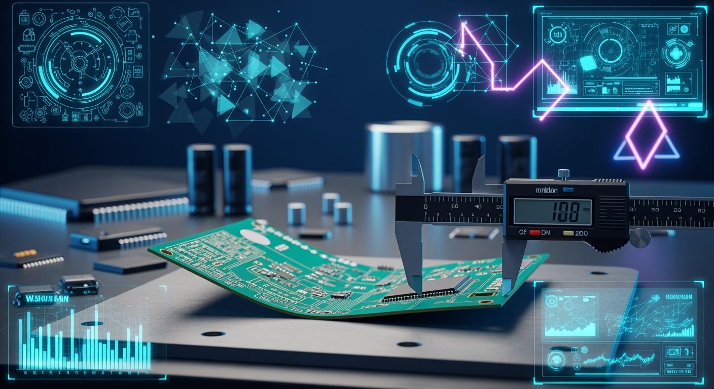
Measurement Techniques
You need to check PCB warpage to keep boards flat and strong. There are many ways to measure warpage. Some use simple tools, and some use special machines. Here is a table that lists the most used measurement techniques:
Measurement Technique | Description |
|---|---|
Feeler Gauge Method | Uses feeler gauges of different thickness to measure warpage between points. |
Height Gauge | Measures height differences between high and low spots for accuracy. |
Contour Gauge | Traces the board’s profile to map its shape and find high and low points. |
Optical Profilometer | Projects light and captures images to create a 3D map of the PCB surface. |
Finite Element Method | Uses strain gauges and computer models to analyze warpage during heating. |
You can also use your eyes, mechanical gauges, CMMs, and laser scanners. Each way has good and bad points.
Contact methods, like feeler gauges and height gauges, touch the board. These ways can miss small bends or twists. They also take longer if you need lots of checks. Non-contact methods, like optical profilometers and laser scanners, do not touch the board. They check the whole surface fast and very well. Non-contact ways are good for boards with tricky shapes or many layers.
Tip: Non-contact measurement does not change the board when you test. You get results faster and more exact, which helps with advanced electronics.
Key Standards (IPC-9641, IPC-6012)
You must follow industry standards for PCB Warpage Testing. Standards tell you what is okay and what is not. Two big standards are IPC-9641 and IPC-6012.
IPC-6012 gives rules for rigid printed boards. It tells you the warpage limits:
Boards without surface mount parts: up to 0.75% warpage.
Boards with surface mount assembly: up to 0.5% warpage.
IPC-9641 is about warpage testing for surface mount technology. It explains how to test and what tools to use.
IPC-TM-650 Test Method 2.4.22 gives steps to measure bow and twist. You use this method to keep your results the same each time.
Other standards, like JEDEC JESD22-B112 and IEC 61189-2, help with special boards, like high-density or car boards.
Here is a table that shows some main standards and their warpage rules:
Standard | Description | Warpage Criteria |
|---|---|---|
IPC-6012 | Rigid printed boards | 0.75% (no SMT), 0.5% (with SMT) |
IPC-TM-650 Test Method 2.4.22 | Bow and twist measurement procedure | Standardized setup for consistency |
JEDEC JESD22-B112 | Surface mount warpage measurement | Temperature-dependent criteria |
IEC 61189-2 | High-density interconnect guidance | Focus on material and warpage performance |
AEC-Q100 | Automotive electronics qualification | Warpage below 0.3% for safety-critical applications |
You can see that standards give clear limits. They help you know if a board passes or fails PCB Warpage Testing.
Warpage Allowance by Application
Not all boards need the same warpage limits. The type of device and how you use the board matter. Consumer electronics, like phones and TVs, can allow more warpage. High-precision devices, like medical or space tools, need tighter limits.
Here is a table that shows warpage tolerance for different uses:
Application Type | Warpage Tolerance Range |
|---|---|
Consumer Electronics | 0.1% to 0.3% |
High-Precision Components | Below 0.05% |
You must check the right standard for your product. For example, IPC-6012 splits boards into classes:
Class 1 (General electronics): up to 0.2% warpage.
Class 2 (Dedicated service): up to 0.15% warpage.
Class 3 (High reliability): up to 0.1% warpage.
Class 4 (Advanced): up to 0.05% warpage.
Note: Using the right standard helps you stop failures and recalls. You make sure your boards work for your customers.
PCB Warpage Testing gives you the facts you need. You can check your results against the standards. You can accept, fix, or reject boards using clear rules. This keeps your products safe and strong.
Warpage Prevention & Control
Design Guidelines
You can stop PCB warpage by making smart design choices. Good design keeps your board flat and strong. Here is a table with important rules you should follow:
Guideline | Description |
|---|---|
Optimized design | Use standard size and weight. Do not make boards too big or heavy. Place V-Cut lines carefully to lower stress. |
Material Selection | Pick strong substrates like FR-4. Use 1.6 mm thickness for balance between strength and cost. |
Proper storage | Do not stack thin panels. Store boards flat so they do not bend. |
Uniform distribution of copper | Spread copper evenly on both sides. This keeps heat even and lowers warpage risk. |
You need to think about the materials you use. Here are some tips:
Choose high-Tg FR-4 (175°C) or low-CTE laminates for boards that get hot often. This helps stop warpage.
Do not mix up the core, prepreg resin, and copper layers. If materials do not match, the board can bend when heated or cooled.
The coefficient of thermal expansion (CTE) for FR-4 is about 14-17 ppm/°C. Copper is about 17 ppm/°C. If these numbers do not match, your board can warp.
High-Tg materials (above 170°C) keep boards strong at high temperatures.
Lower CTE-Z values mean less expansion up and down, which helps control warpage.
Tip: Use design software to check for heat problems. Add dummy copper fills in empty spots to keep the board balanced.
Manufacturing Best Practices
You can control warpage during manufacturing by following good steps. Here are some things you should do:
Use designs that follow standard size and weight rules. Place V-Cut lines to avoid weak spots.
Pick strong materials like fiberglass-reinforced FR-4. This lowers the risk of warping.
Store thin panels flat. Do not stack them. This keeps them from bending before assembly.
Make sure copper foil is spread evenly on both sides. This helps the board heat and cool evenly.
Post-bake treatment is important. After pressing layers together, put the board flat in an oven at 150°C for four hours. This step lets the board release stress and cures the resin fully. Baking the board before or after cutting removes moisture and makes the resin solid. Bake at 150°C for 8±2 hours before cutting the copper clad laminate. This keeps the board thickness even and lowers warpage risk.
When you pick a supplier, look for these things:
Balanced designs that stop warpage.
Good heat management during production.
Careful storage to keep boards flat.
Materials with matching CTE values.
High-Tg FR-4 or polyimide for boards that face high heat.
Uniform laminate thickness. Thicker boards warp less.
Symmetrical copper layers. Use design tools to check for warpage risks.
Add dummy copper fills in areas with few traces.
Note: Following these steps helps you avoid defects during assembly. You get better yield rates and save money by reducing rework and scrap.
Quality Assurance
You need strong quality checks to keep warpage under control. Ongoing PCB Warpage Testing helps you catch problems early. Here is what you should do:
Check for parts that are not lined up. Warped boards can move parts and cause open circuits or shorts.
Watch for bad solder joints. Warpage can make soldering uneven, leading to weak connections.
Look for mechanical stress. Warped boards can crack parts and cause solder fatigue over time.
Here is a table with common quality assurance steps:
Protocol Type | Description |
|---|---|
Design Optimization | Use mirror symmetry, balance copper density, and avoid large copper pours on one side. |
Material Selection | Pick high-Tg FR-4 or low-CTE laminates. Make sure resin content and glass weave are consistent. |
Manufacturing Process Control | Use precise temperature and pressure during lamination. Cool boards slowly to release stress. |
You should test boards at every stage. This keeps your products reliable and lowers the risk of failure. If you stop warpage, you will see fewer defects and higher yield rates. Even a small drop in defects can save thousands of dollars in mass production. You also avoid warranty claims and customer returns, which protects your reputation and saves money.
Remember: Good warpage prevention means fewer repairs, better reliability, and happier customers.
You help make devices work well by testing for PCB Warpage at every step. If you follow rules and good ways to build, you can stop warpage and make better boards. The table below shows how picking the right design and handling stress helps devices last longer:
Cause | Reliability Solution |
|---|---|
CTE mismatch | Use compatible materials and underfills |
Stress redistribution | Select low modulus underfill for solder joints |
Make your design even on both sides.
Pick strong and good materials.
Watch the building steps closely.
Check boards with smart machines.
If you test for warpage often, you will have fewer broken boards and less need to fix or recall them.
FAQ
What tools do you need for PCB warpage testing?
You can use feeler gauges, height gauges, contour gauges, or optical profilometers. Non-contact tools like laser scanners give fast and accurate results. Choose the tool that matches your board type and your testing needs.
How often should you test for PCB warpage?
You should test at every key stage: after fabrication, before assembly, and after soldering. Regular checks help you catch problems early and keep your boards reliable.
Can you fix a warped PCB?
You cannot always fix a warped PCB. Sometimes, baking the board can help release stress. If the warpage is too much, you should reject the board and use a new one.
Why do standards matter in PCB warpage testing?
Standards give you clear rules for what is acceptable. They help you decide if a board passes or fails. Following standards keeps your products safe and trusted.
See Also
Evaluating Advanced HDI PCB Technologies for Future Electronics
Essential Guidelines for Designing PCB Circuit Boards
Addressing Common PCB Design Issues in SMT Processing