Advanced PCB Thermal Management Design for High Power
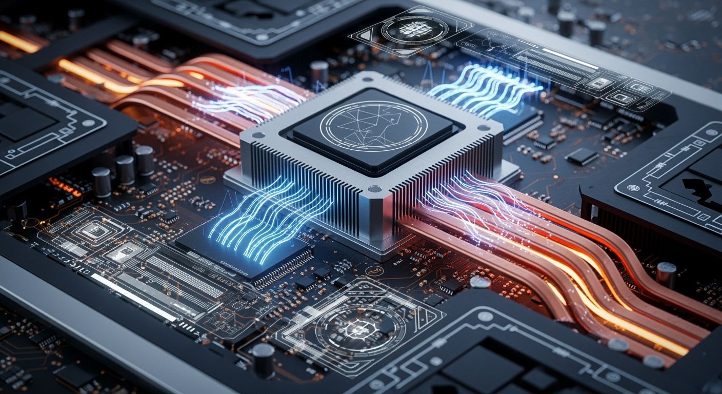
High-power circuit boards get very hot when they are working. You need to use advanced pcb thermal management to move this heat away from delicate silicon parts. Your main goal is to spread heat across the board's copper layers before it releases into the air. Improving your copper layout reduces thermal resistance along important pathways. Different cooling methods handle various heat levels in high-power electronics.
Cooling method | Range (W/m²) |
|---|---|
Air-cooling | up to 500,000 |
Liquid-cooling | over 1,000,000 |
Industrially feasible high-heat-flux cooling | 5,000,000 – 10,000,000 |
Using this thermal design guide helps your high-power systems stay reliable over time through smart pcb thermal design.
Key Takeaways
Copper layers and special base materials move heat away from fragile electronic parts very well.
Thick copper paths and wide metal areas lower electric resistance and stop dangerous hot spots.
Groups of heat-conducting holes filled with copper paste move internal heat straight to the outside layers.
Heat sinks, thermal interface materials, and cooling coatings protect high-power circuits under heavy workloads.
Core Fundamentals of PCB Thermal Management
Heat Flux Conduction and In-Plane Spreading
A high power pcb works as the main heat sink for your circuit. Parts make tiny hot spots right where they attach to the board. High power pcb design relies on copper layers to pull heat away from active silicon. Copper traces and solid planes push heat sideways across the board material. Spreading heat across the board lowers total thermal resistance and creates a smooth surface temperature.
You can control this heat spread by changing a few physical parts. Picking thicker copper instead of thin copper gives heat much wider paths to flow through. Thicker copper planes also stop high currents from losing energy as heat inside traces. Choosing better substrate materials and adding thermal vias helps heat move straight down. Good planning moves extra heat to cooler areas before it ruins pcb performance.
Natural Convection and Radiation Mechanisms
Once heat spreads across the board, it must escape into the surrounding air. Heat leaves solid circuit boards through different natural pathways. You can use this thermal design guide to balance all your main cooling paths.
Mechanism | Relative contribution | Dominance factors |
|---|---|---|
Conduction | Dominates within the high power pcb structure | Copper distribution, via density, substrate choice |
Natural convection | Primary once heat reaches the board surface | Board orientation, component layout, surrounding air |
Radiation | Minor under normal operating conditions | Surface temperature above 100°C significantly |
Conduction carries most of the heat inside the board and copper layers. Convection takes over as soon as heat reaches the outer surfaces. Warm air moves up naturally, soaking up heat and carrying it away from hot spots. The way you mount your board changes how well convection works. Mounting the board upright lets rising air sweep easily across both sides. Heat radiation provides very little extra cooling during normal board use. Smart cooling plans focus on conduction paths and surface air flow to keep systems working well. Following this thermal design guide helps you improve high power pcb performance during heavy use. Taking the right high power pcb design steps protects delicate parts so they last much longer.
High Power PCB Substrates and Material Selection
High-Tg FR-4 vs Metal Core PCBs
You must pick the right base material to control thermal stress in strong electronics. Standard FR-4 offers a low thermal conductivity value of ~0.3 W/m·K. High-Tg FR-4 conducts heat similarly, but it adds structural stability when warm. You should check four key material traits:
Glass transition temperature (Tg): Higher Tg keeps the board firm during high temperature use.
Decomposition temperature (Td): High Td prevents lasting chemical damage while soldering.
Coefficient of thermal expansion (CTE): Low Z-axis stretch protects vias from cracking under stress.
Thermal conductivity (k): Higher dielectric k improves your overall heat transfer directly.
A high power pcb needs a steady path to draw heat away from active parts. Metal core circuit boards place aluminum under a thin dielectric layer. This solid metal sheet moves heat from high current pcb traces faster than FR-4. Thermally conductive FR-4 hits 0.6–1.0 W/m·K, but metal boards work much better. Adding metal inside your high power pcb design stops hot spots during heavy work. A good high power pcb keeps low thermal resistance across all board layers.
Ceramic and Polyimide Substrate Capabilities
Ceramic boards give top cooling support for very active high power pcb builds. Alumina ceramic provides a strong thermal conductivity of 20–35 W/m·K. Aluminum nitride ceramic hits 140–180 W/m·K to push high heat across layers. These smooth ceramic items remove organic dielectric walls completely. Heat travels right through the substrate into the air to save your high power circuits. Every custom high power pcb relies on these simple paths to drop board heat.
You can craft a tiny high current pcb using bendable polyimide or hard ceramic materials. Polyimide takes heavy heat well while keeping its structural strength intact. Choosing ceramic parts in your high power pcb design removes hard thermal paths entirely. Wise material choices protect every high power pcb during long daily tasks. Top design teams use ceramic options to boost each high power pcb design setup. A great high power pcb manages intense heat while keeping peak electrical performance.
Effective PCB Thermal Design via Copper Layout
Heavy Copper and IPC-2152 Trace Sizing
High current pcb paths create extra warmth from basic electrical resistance losses. Using thicker trace metal lowers this internal resistance directly, reducing unwanted heat during use. Standard 1 oz copper sits at roughly 35 µm thick, while heavy 3 oz copper measures near 105 µm. Tripling this cross-sectional area lets circuits carry much more power while holding low temperature increases.
Switching from 1 oz to 3 oz copper expands conductor area to move heat away from active component pins fast.
Engineers must size board traces using modern IPC-2152 rules instead of old IPC-2221 math. The IPC-2152 standard uses real charts considering copper weight, board thickness, and surrounding air space.
Feature / Standard | IPC-2221 | IPC-2152 |
|---|---|---|
Deriving capacity | Uses a single conservative formula | Uses empirical charts and correction factors |
Trace location factor | Treats internal traces conservatively | Models specific layer placement and local thermal environment |
Modern stackup optimization | Over-sizes trace widths | Permits optimized trace widths through precise thermal modeling |
Doubling copper thickness boosts total trace current capacity by 60–100% for the same heat target. For example, a 1 mm wide trace using 2 oz copper handles 4.2 A at a 10°C rise, versus 2–2.5 A for 1 oz copper. Modern IPC-2152 testing proves inner traces handle almost as much current as top layers near copper pours. You should widen middle traces and place nearby copper sheets whenever high-power lines run inside the board.
Plane Strategy to Minimize I2R Losses
Solid copper sheets serve as low-resistance bases for every high power pcb design. You must keep high current paths wide and short to stop energy loss. Utilizing large continuous copper pours over thin traces drops current density and stops hot spots.
Put solid power and ground layers next to each other to drop loop inductance and reduce return path resistance.
Shape large copper planes using IPC-2152 current limits so high heat does not bend your board.
Spread hot parts evenly across your circuit layout instead of grouping them together in one place.
Link large copper areas through several layers with via groups to keep electrical voltage stable everywhere.
Place thermal vias right under hot MOSFETs, ICs, and regulators to send heat to inner copper layers.
Continuous copper planes drop total DC resistance, saving your high power circuit from sudden voltage drops. Every high power pcb layout needs heavy copper coverage across all internal layers. Adding small split planes in tight spots adds unwanted inductance, so compact boards need big via farms for connections.
Using this total thermal design guide guarantees solid performance under heavy power loads. Modern layout planning balances trace shapes, copper weight, and board layer stacks carefully. Applying these layout steps turns your high power pcb into a cool, reliable electronic system. Smart design habits protect sensitive parts when power demands reach their absolute peak. Every good pcb thermal design uses these core rules to build tough electronics that last.
Thermal Via Array Design and Micro-Via Rules
Via Array Pitch and Dimensional Rules
You must place thermal via arrays directly beneath component pads to move heat away from active junctions. Thermal via arrays do not lower the intrinsic junction-to-case resistance of a component package. Instead, these arrays create parallel thermal pathways that reduce the case-to-board resistance across your substrate. Designing a high power pcb requires precise structural parameters to maximize vertical heat conduction.
Parameter | Recommended value | Thermal effect |
|---|---|---|
Finished hole diameter | 0.2 mm to 0.35 mm | Controls internal barrel surface area and solder wicking risks |
Center-to-center grid pitch | 1.0 mm to 1.2 mm | Prevents board structural weakening while supporting uniform heat flow |
Moderate heat density | 8–12 vias per square centimeter | Provides baseline cooling for standard thermal pads |
High heat density | 20 or more vias per area | Lowers thermal resistance for components dissipating over 5 W |
You achieve optimal thermal spreading by arraying small micro-vias under component pads. A high-density array uses 20–50 vias per pad for demanding high power pcb design setups. Smaller hole sizes permit more vias within a tight space. However, spacing vias closer than 1.0 mm can weaken mechanical structural strength. You should maintain regular grid spacing to optimize heat transfers into internal plane layers. A solid high power pcb layout uses thermal arrays to drop temperature gradients.
IPC-4761 Via Filling and Capping Methods
You must select proper barrel treatment methods to maintain physical electrical reliability. Unfilled vias leave air pockets inside board structures. Air exhibits a low thermal conductivity of ~0.3 W/m·K, acting as a thermal insulator. Unfilled vias can also wick solder during component assembly, reducing direct surface contact.
Unfilled vias create an air gap between the component pad and heatsink layer. This air gap has thermal conductivity 600 times worse than copper. A 50% filled via array can increase junction temperature by 18–22°C above predictions. Each plated via contributes about 33°C/W for a standard 1.6 mm board with 25 μm copper plating.
Standard IPC-4761 via filling specifications solve these assembly issues while improving performance. Filling vias with copper paste raises effective thermal conductivity to 8 W/m·K. This treatment delivers more than 25 times higher heat transfer than air. A copper-paste filled via array reduces maximum component temperatures by 22°C in a high power pcb assembly.
Plated-only unfilled vias provide basic thermal paths but suffer from solder wicking issues.
Non-conductive filled vias seal the hole to prevent solder migration into lower layers.
Conductive filled vias lower thermal resistance by 35–65% across board thermal pads.
Capped via-in-pad structures place planar copper over filled vias to create smooth soldering surfaces.
Using filled vias under pads on a board thicker than 0.7 mm drops thermal resistance by up to 20% compared to open holes. Capped via-in-pad architectures eliminate solder loss during reflow soldering. This design choice maintains strong mechanical bonds under every high power pcb component. Every high power pcb thermal architecture relies on dense via farms to pull heat toward outer ground layers. You must plan via structures carefully within your high current pcb routing scheme. Dedicated copper fills protect your high current pcb planes from localized heating. Following these IPC-4761 structural rules optimizes high power pcb design reliability across long product lifetimes.
Advanced Thermal Management Techniques and Mechanical Cooling
Heat Sinks TIMs and Surface Attachment
You need mechanical cooling methods when copper layers cannot remove extra part heat. Metal heat sinks pull warmth right away from active circuit parts. Strong fans create fresh air streams that sweep off trapping heat layers. Fan ducts cool hot processor chips by 15–20°C over basic setups. Small heat pipes move thermal energy using inner liquid boiling cycles. Bathing boards in special liquid drops heat by 25% easily.
Tiny surface bumps create empty air pockets between metal sinks and parts. You must press surfaces tight to drop contact resistance across the board. Spring screws keep steady squeeze force between 20 and 50 psi. Etched heat sink surfaces must stay flatter than 0.050 mm total. Thermal interface materials fill air gaps so parts stay cool always.
Thermally Conductive Conformal Coatings
Clear protective coatings shield circuit boards from moisture, dirt, and electrical shorts. Common acrylic, silicone, epoxy, or plastic coatings trap heat like thermal insulators. These base layers measure very low thermal conductivity near 0.1–0.3 W/mK. You can pick special cooling coatings to boost heat transfer naturally. Adding ceramic or metal fillers raises thermal conductivity up to 1–3 W/mK. Good thermal planning keeps heavy power boards safe under hard work.
Modern coating materials speed heat flow while protecting every delicate board pad. Special Shin-Etsu silicone formulations reach 0.1–5.0 W/mK conductivity under careful application. Multi-layer coatings from 3M offer 0.8–3.5 W/mK through added ceramic particles. These improved coatings boost heat transfer up to 50 times better. Spreading heat-conductive coatings over your board protects traces while lowering junction temps. Every strong circuit board needs targeted coating protection for long reliable service.
Simulation Workflows and Manufacturing Validation
Thermal Management Co-Simulation
You run electrothermal co-simulation to guess component junction heat before building your circuit board. Modern thermal tools combine electrical power loss directly with heat flow solver engines. Doing a detailed thermal analysis helps you spot hot areas before making physical board prototypes. Programs like Celsius Studio run complete thermal models using small mesh grids and layered stackup data. You track temperature-based trace resistance and self-heating inside one simple process. Using a thorough thermal design guide ensures your high power pcb design keeps safe heat limits during daily tasks.
Testing conditions like airflow, case contact, and warm-up times gives you real results. Top simulation tools adjust designs using IPC-2152 trace rules to stop heat spikes.
A TCAD-based electro-thermal co-design framework (Silvaco Atlas) solves electrical and thermal physics together before making any board mask.
DFM Constraints and Verification Checklist
You must follow strict factory rules to keep board quality high and avoid production errors. High power pcb design needs full reviews for heavy copper layers and dense thermal vias. Your DFM checks must cover hole sizes, metal rings, trace gaps, solder masks, cooling features, and part locations. You should link thermal vias to inner planes with solid copper instead of thermal relief spokes. Matching via fill expansion rates with the board material stops barrel cracking during hot cycles.
You check test boards after making them through tough thermal checks and stress tests. Burn-in tests run boards under high heat and strong voltages for long hours to catch early flaws.
Validation Check | Required DFM Action | Manufacturing Effect |
|---|---|---|
Pad via filling | Use IPC-4761 Type VII capped fills inside SMT pads | Prevents solder wicking and weak solder joints |
Stress testing | Perform thermal shock tests and solder float tests | Validates via barrel integrity under severe temperature shifts |
Following these practical rules completes your thermal design guide for mass factory builds. Checking accurate thermal models before production prevents costly layout redesigns. Using steady-state thermal tests during design checks secures strong high-power product releases.
You create a great heat path by picking thermal substrates, adding thick copper, and using dense via groups. Achieving effective pcb thermal design requires you to balance material selection, factory rules, and thermal simulation early in your planning workflow. Good thermal management stops board damage and protects high power circuits.
Validation Metric | Reported Parameter / Threshold | Purpose Before High-Power PCB Release |
|---|---|---|
Hotspot detection | Flag simulated temperatures above 85°C | Identify areas requiring thermal mitigation |
Junction temperature | Keep semiconductor junction below 125°C | Avoid premature lifespan degradation |
You must check performance using thermal simulation before sending files to factory builders. This last test ensures total pcb thermal management success.
FAQ
What hole size and pitch should you choose for thermal via arrays?
Aim for finished hole sizes between 0.2 mm and 0.35 mm. Space the hole centers 1.0 mm to 1.2 mm apart in a grid layout. This pattern keeps the board strong and helps heat move straight down evenly.
How does copper paste filling improve thermal via performance?
Empty holes trap air, which blocks heat with a low 0.3 W/m·K flow rate. Filling the holes with copper paste using IPC-4761 steps boosts heat flow to 8 W/m·K. This simple upgrade lowers top part temperatures by 22°C. Check our thermal design guide to improve your board layer setups.
Why should you use IPC-2152 instead of IPC-2221 for trace sizing?
Old IPC-2221 math relies on safe guess rules that make trace lines way too wide. Modern IPC-2152 rules use real test charts based on board thickness, metal weight, and nearby room air. Using this thermal design guide helps you size trace lines right through smart heat modeling.
When must you apply advanced pcb thermal management to your layout?
Use advanced pcb thermal management when hot parts push out more heat than basic board surfaces can vent away. Using metal bases, ceramic parts, filled holes under pads, or outer cooling fins keeps internal chip joints below safe temperature limits.
See Also
Unlocking Thermal And Electrical Efficiency With Aluminum Printed Circuit Boards
How To Design Exceptional High Performance PCBs For LED Lighting
Crucial Design Strategies For Heavy Copper High Current Circuit Boards
Solving Frequent SMT Assembly Challenges In Modern Printed Circuit Design
Benefits And Uses Of Thermoelectric Separation In Copper Based PCBs
