Any-layer HDI PCB manufacturing technology
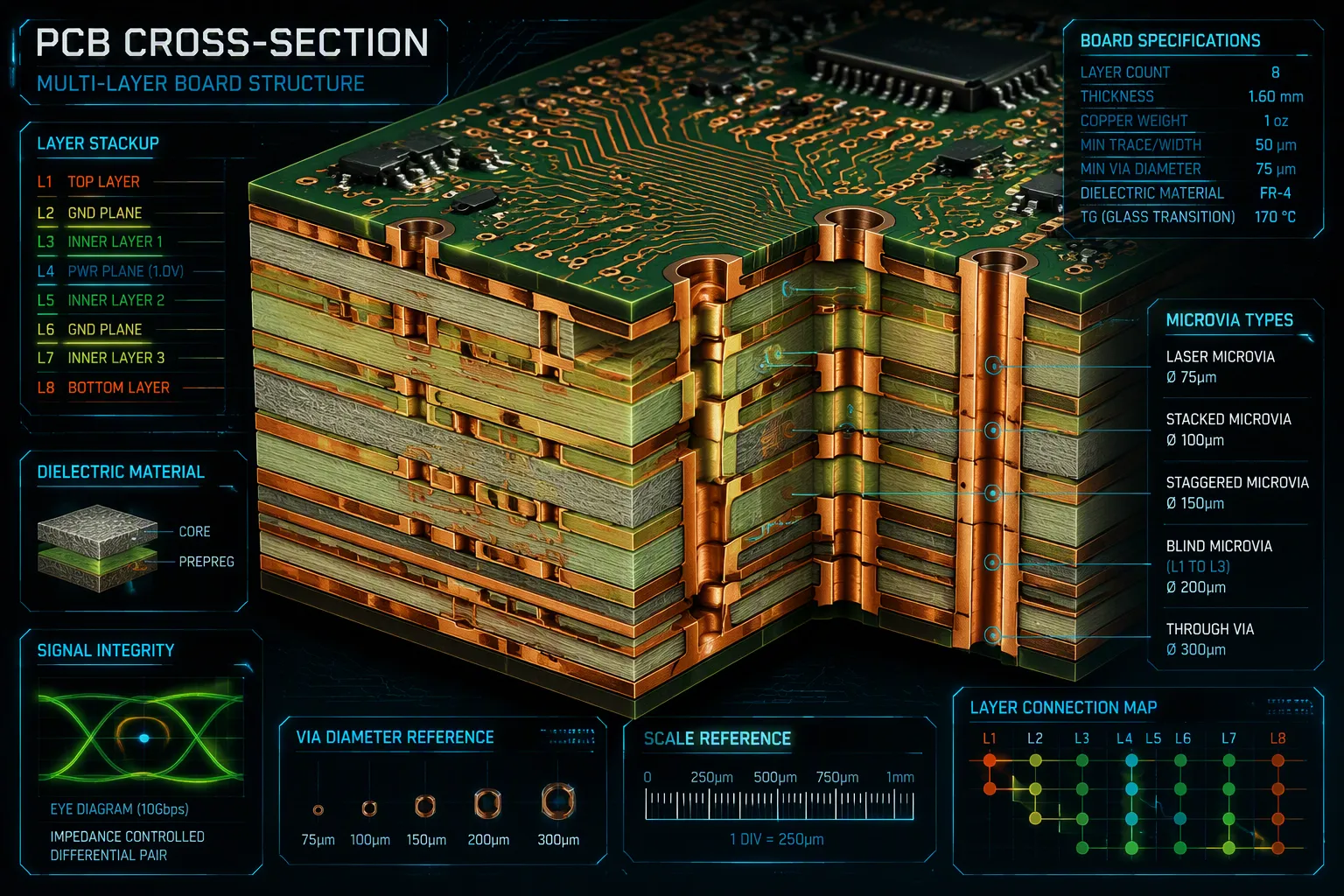
An any-layer HDI PCB connects every layer using copper-filled stacked microvias. This high-density interconnect technology achieves maximum routing density. You can route dense BGA packages with ease. Thin dielectrics, as low as 0.1 mm (approximately 4 mils), reduce board thickness significantly. How far can miniaturization go? This technology answers that question directly. Your HDI PCB design gains freedom to place vias anywhere on any layer. The HDI manufacturing process uses sequential lamination for each layer. Every circuit layer links directly to others. This HDI PCB design approach eliminates traditional routing limits. Manufacturing complexity increases, but density rewards you. Your HDI board integrates multiple functions into one compact unit. The interconnect structure supports today's demanding electronics.
Key Takeaways
Any-layer HDI PCBs use copper-filled stacked microvias to connect every layer, allowing for very dense routing and more design freedom.
This technology can handle BGA pitches as small as 0.25 mm, making it perfect for compact, powerful electronics.
The manufacturing process uses step-by-step lamination and exact laser drilling, so you must pick materials carefully and design the board so it's easy to build.
Any-layer HDI can cut board layers by 30-50% versus standard HDI, making boards thinner and smaller.
To succeed, work with an experienced maker early on to check your stackup and design rules, so the move to production goes smoothly.
What Is an Any-Layer HDI PCB?
An any-layer HDI PCB removes all old routing limits. In this design, every layer can connect to any other layer freely. You can put a via anywhere on any layer. Wires from one layer can link straight to wires on another layer. This total freedom to connect is what makes it different from regular HDI stackups.
The key is copper-filled stacked microvias. These tiny parts create vertical paths through the board. Each microvia goes through one dielectric layer. Lasers drill the micro via holes with great accuracy. Then copper fills each hole completely. This makes a strong solid pillar. You can stack these pillars over many layers. The result is a smooth vertical link through the whole board.
Copper-Filled Stacked Microvias Explained
Making these microvias needs careful work at every step. First, a CO2 or UV laser removes the dielectric material. This makes the microvia hole, usually 0.075 mm to 0.15 mm wide. Next, the process cleans the hole to take off resin leftovers. Then electroless copper deposition coats the via walls with a thin copper layer. Finally, electroplating fills the via solid with copper. This creates a flat, conductive surface for the next build-up layer.
The table below shows typical specs for these structures:
Parameter | Typical Specification |
|---|---|
Microvia diameter | 75–150 µm |
Microvia aspect ratio | 0.8:1 to 1:1 (max) |
Recommended stack height | 3–4 microvias per column |
Capture pad diameter | 250–350 µm (for a 100–150 µm via) |
Layer-to-layer registration tolerance | ±25–50 µm per layer |
Thermal conductivity of copper-filled stacked via array | 100–200 W/mK |
The copper filling uses advanced electroplating methods. Pulse plating gives void-free, high-density copper-filled stacked microvias. The grain structure stays even throughout. Multi-stage lamination controls pressure, heat, and resin flow. This makes sure layers stick together well. Plasma desmear and special chemical treatments improve copper adhesion. During production, cross-section analysis, AOI, and X-ray checks confirm quality.
Key Benefits for High-Density Designs
This technology allows amazing board integration. You can combine the jobs of many separate PCBs into one small board. Full layer-to-layer links remove old via limits. You place parts freely and route densely. The result cuts routing layers and board size while keeping performance.
The electrical gains are big. Shorter links give stronger signals. You get about ten times lower via electrical parasitic. Fewer stubs improve signal quality. Steady voltage rails keep power delivery stable. Less crosstalk and noise protect sensitive circuits. Much lower RFI and EMI cut interference. Closer ground planes improve shielding. You also get chances for distributed capacitance between power and ground layers.
Increased electrical performance – shorter interconnects, stronger signals
For dense BGA packages, this design works great. You can fan out under the BGA without dog-bone routing. The interconnect density reaches levels impossible with standard HDI. Your high-density interconnect structure supports today's demanding electronics. The hdi manufacturing process delivers boards that integrate multiple functions into one unit. This reduces assembly complexity and connector count significantly. Your hdi pcb design gains unmatched flexibility. The pcb becomes a single, efficient platform for complex circuitry.
Any-Layer HDI PCB vs. Standard HDI Stackups
Standard HDI stackups use numbered notation. A 1+N+1 stackup has one build-up level on each side of a core. A 2+N+2 stackup adds two levels per side. The pattern continues to 3+N+3 and 4+N+4. Each pair increases capacity. But these designs limit where you place vias. The core restricts connections. You must route through the core.
Any-layer designs remove the core. You place microvias in any layer of the board. This changes the routing. The hdi manufacturing process uses sequential lamination. Each layer gets its own via step. The process repeats for every layer. This gives total freedom. The hdi pcb design for complex circuits becomes simpler. The lamination process controls temperature. The plating process fills the vias.
From 1+N+1 to 2+N+2 and Beyond
The first number is build-up levels on top. N is the core count. The third number is build-up levels on bottom. A 1+N+1 board has one level on each side. A 2+N+2 board has two. Each level adds one microvia tier. The vias in these levels stack or stagger. They connect to the core. The core limits the connection paths.
The any-layer design removes this limit. You stack microvias through all levels. The vias form continuous columns. This supports extreme routing. The design process becomes more flexible. You route signals between any two levels. The hdi pcb design benefits. The drilling process creates the holes. The registration process must be precise.
Why Choose Any-Layer Over Other HDI Types?
The main advantage is dense BGA routing. Standard HDI stackups struggle with fine-pitch BGAs. Any-layer HDI handles pitches as low as 0.25mm. The copper-filled stacked microvias make this possible. You eliminate the through-hole core. This opens space under the BGA.
Any-layer HDI PCBs can accommodate BGA pitches as low as 0.25 mm by utilizing copper-filled stacked microvias and eliminating the traditional through-hole core.
The trade-off involves cost and complexity. The hdi manufacturing process requires more steps. Each level needs its own lamination. The process demands registration. Fabrication costs rise. But you gain density and signal integrity. Shorter connection paths reduce loss. The board thickness decreases. Performance improves. The stacked vias handle current loads.
Any-layer HDI (also known as ELIC) is used for extreme miniaturization and the highest density routing, which is essential for routing dense BGA packages with very fine pitch.
You choose any-layer HDI when density is the priority. The hdi fabrication process delivers boards that others cannot produce. The design flexibility justifies the cost. For extreme miniaturization, this is the only option. The high-density interconnect makes it the best choice. The any-layer hdi pcb meets the highest demands.
Manufacturing Process for Any Layer HDI PCB
The hdi manufacturing process for any-layer boards follows a precise sequence. Each layer gets its own via metallization, filling, and plating before stacking. This step-by-step method builds the board one level at a time. The whole process needs exactness.
Sequential Lamination and Via Formation
You start with a rigid core. This core usually has 2-8 layers of FR-4 or high-Tg material with a glass transition temperature of at least 180°C. Inner layers get imaged, etched, and checked through automated optical inspection.
The sequential lamination process follows these steps:
Via Plating and Fill: Drill buried core via holes. Apply electroless copper deposition followed by electrolytic plating. Fill vias with conductive or non-conductive material and smooth the surface.
First Build-Up Film Lamination: Laminate thin HDI build-up film and copper foil onto the core sub-stack. Image and etch to form circuits.
Laser Drilling: Use UV lasers at 355nm to drill microvias into the build-up film. These holes end on the same layer as internal buried vias.
Microvia Plating: Plate the microvia holes to form the first set of laser-drilled vias. This bonds them to the exposed pad and copper film.
Next HDI Lamination: Add more build-up film layers. Repeat steps 1-4 for each new layer. For stacked vias, add a fill, plate, and planarize step.
Through-Hole Via Processing: Drill and plate traditional through-hole vias. Apply final surface finish such as ENIG or immersion silver.
Each lamination cycle runs at controlled temperature between 180-200°C and pressure of 200-300 psi. The process keeps alignment tolerance of ±0.002 inches through X-ray registration. This precision matters because each layer must align perfectly with the one below. The plating process fills the vias completely. Any misalignment at this stage creates defects that spread through the stack.
Material Selection and DFM Guidelines
Thin dielectric layers reduce overall board thickness. You can use dielectrics as low as 0.1 mm (approximately 4 mils). FR-4 remains a common cost-effective choice for many designs. High-Tg materials work better for boards that face thermal stress during assembly.
Design for manufacturing starts with via aspect ratios. The aspect ratio compares via diameter to dielectric thickness. A 100µm diameter via in a 100µm dielectric gives a 1:1 ratio. This ratio represents the IPC maximum limit. This design process requires careful planning.
Aspect Ratio | Recommendation |
|---|---|
Target for standard production | ≤0.75:1 |
IPC maximum limit | 1:1 |
Benefit of lower ratio | Improves plating uniformity, reduces voids |
You should use the largest feasible drill diameter for your design. Maintain uniform dielectric thickness across the board. These practices improve copper fill uniformity and prevent void formation. The vias form continuous columns through the stack.
First-pass yield rates for 12-layer any-layer boards typically range from 88-92%. Process optimization can push this higher. One manufacturer reported 91.5% first-pass yield after improvements. Your fabrication partner should share their yield data and process controls. This process transparency helps you plan.
The hdi pcb design must account for these manufacturing realities. Plan your stackup early. Consult with your fabricator before finalizing the design. This collaboration ensures your any-layer hdi pcb meets both performance and manufacturability goals. The high-density interconnect structure rewards careful planning. This density enables the routing freedom you need for complex designs. Shorter connection paths improve signal integrity. Your pcb fabrication success depends on following these guidelines from the start.
Designing and Ordering Your Any-Layer HDI PCB
Now you know how the board is made. The next step is to design your board and get it made. You need to guess the right number of layers. A good rule: any-layer HDI can reduce the number of layers compared to normal HDI. But you must check your stackup with the maker early. This makes sure your design follows the rules and avoids costly fixes.
Determining the Right Layer Count
Start with your pin density and how complex the wires are. Follow these steps to find the layer count:
Trace sizing: Use the BGA pitch to set the max trace width. Then find the layer thickness needed for the wanted trace impedance. This gives you a controlled impedance trace that fits in the routing channels.
Nets per layer estimate: Choose trace width and spacing. Guess your board size. Multiply the number of BGA breakout channels per area by the board area. This gives you the number of nets you can route on one layer.
Layer count calculation: Divide your total net count by the nets per layer. This gives you the number of signal layers. Then add power and ground planes to get the total HDI PCB stackup layer count.
Remember that any-layer HDI gives you more routing channels per layer than standard HDI. The layer reduction is real for dense designs. Use the maker's design rules to check your numbers.
Preparing Your Design Files for Fabrication
Your fabrication files must have all details. The maker needs to check many stackup settings. The table below shows the key settings to confirm.
Stackup Parameter | Validation Requirement | Engineering Justification |
|---|---|---|
Build-up layers | Make sure each new layer helps with a specific routing or connection need | Stops extra manufacturing steps and complex alignment |
Dielectric materials | Agree on material type, thickness, and resin behavior | Affects laser drilling, lamination quality, and impedance control |
Copper specifications | State base and final copper weight per layer | Sets trace shape and plating allowances during making |
Reference planes | Ensure critical signals have steady return paths | Avoids return current breaks that hurt signal quality |
Via spans | Check every laser, buried, and through-hole span matches the layer build | Prevents CAM errors and wrong electrical connections |
Finished board thickness | Define normal thickness and tolerance for the full board | Core thickness alone is not enough; the full stackup sets final board size |
Include via specs, impedance needs, and any other notes in your fabrication notes. Ask the maker to send back a proposed production stackup before final routing. This stops last-minute changes that affect trace widths. Working early with your hdi pcb design partner helps a smooth move from idea to production.
Any-layer HDI PCB technology delivers the ultimate solution for extreme density. Copper-filled stacked microvias enable free interconnection between every layer. You achieve unmatched design flexibility for dense BGA routing. Your hdi pcb design gains routing freedom. Board thickness reduces significantly. Signal integrity improves.
Higher cost and complexity come with this technology. The rewards outweigh these trade-offs. Your hdi pcb design pushes the limits of what a circuit can achieve. Each layer connects directly to others.
Consult an experienced manufacturer early in your design phase. Validate your stackup and design rules together. This partnership ensures a smooth transition from concept to production. Your pcb fabrication partner becomes an innovation ally. You push the boundaries of innovation.
FAQ
How does any-layer HDI differ from standard HDI?
Standard HDI limits vias to build-up layers. Any-layer HDI places vias on any layer. You gain full routing freedom. This hdi design handles dense BGA packages. Your pcb becomes smaller and thinner.
What BGA pitch does any-layer HDI support?
Any-layer HDI supports BGA pitches as low as 0.25 mm. The high-density interconnect structure uses copper-filled stacked microvias. You eliminate the through-hole core. This opens routing space under the BGA.
What is the typical yield rate for production?
First-pass yield for 12-layer any-layer boards ranges from 88% to 92%. Process optimization improves this rate. Ask your fabrication partner for their yield data. This helps you plan production.
How do I choose the right layer count?
Start with your pin density. Calculate trace width from BGA pitch. Estimate nets per layer. Divide total nets by that number. Add power planes. This design process helps you find the right layer count. Any-layer HDI can reduce layers.
See Also
Design And Production Of Any Layer HDI Circuit Boards
Explore Modern HDI PCB Prototyping Methods Now
Advantages Of LDI Exposure Equipment For HDI PCB Fabrication
Essential Design Factors For Reliable HDI PCB Production
Manufacturing Techniques For Heavy Copper Multilayer Circuit Boards
