HDI PCB Design Basics for Entry-level Engineers

You see high-density interconnect as a big change in printed circuit board technology. HDI PCB basics help you learn how these advanced printed circuit boards can fit more things into smaller spaces. The good things include using less material and building faster. Many engineers pick HDI PCB design for smartphones and new devices. The table below shows how fast the market is growing:
Year | HDI PCB Market Size (in billion USD) | Growth Rate (%) |
|---|---|---|
2023 | 12.5 | - |
2032 | 23.8 | 7.1 (maybe over 10) |
You get good things like easier device design and better performance when you learn HDI PCB basics.
Key Takeaways
HDI PCBs let you fit more parts in small spaces. This makes them great for new devices like smartphones and wearables.
You need to know about microvias, blind vias, and buried vias. These help keep signals strong and make the board smaller.
Always pick the right materials and follow the rules. This helps your HDI PCB work well and last longer.
Plan your design with care, like trace width and via size. This stops common problems and makes your board work better.
Join online groups and use resources to learn more about HDI PCB design. This will help you do better on your projects.
What is HDI PCB?
High-Density Interconnect Overview
High-density interconnect is a new way to design circuit boards. HDI technology lets you put more parts in a small space. You can use HDI PCB to make boards that are light and small. These boards are special because they use blind and buried vias, coreless builds, and passive substrate builds. These things make HDI PCB different from regular PCB designs. You get better performance and stronger boards. You can also make products faster.
Parameter | Standard PCB | HDI PCB |
|---|---|---|
Size and weight | Large and heavy | Small and light |
Component density | Lower | Higher |
Via technology | Through hole, blind, and buried vias | Blind, buried, and micro vias |
Aspect ratio | Higher | Lower |
Compatible to high pin count devices | May or may not | Yes |
Compatible to small pitch devices | May or may not | Yes |
Number of layers | More | Less |
Drilling technology | Mechanical drilling | Laser drilling |
Tip: HDI PCB technology helps you make fast and tiny devices.
Key Features: Microvias, Blind & Buried Vias
HDI PCB has many features that help you fit more parts. Microvias are very small holes that link layers together. Blind vias join the outside layers to the inside layers. Buried vias only join the inside layers. Laser drilling is used for microvias. This makes the holes very exact.
Via Type | Diameter | Pad Diameter | Aspect Ratio | Maximum Depth |
|---|---|---|---|---|
Microvia | <0.15 mm | <0.35 mm | <1/1 | 0.25 mm |
Buried Via | 0.15 mm (min) | N/A | 6:1 (recommended) | N/A |
You can look at the chart to see how standard and advanced microvias are not the same.
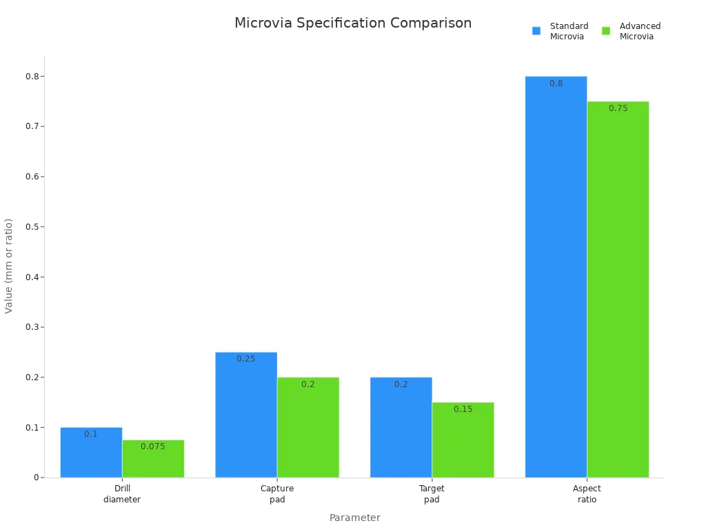
These features let you make boards for things with lots of pins and tiny parts.
HDI PCB Applications
HDI technology is used in many fields. People use high density interconnect in phones, tablets, and smartwatches. Cars use HDI PCB for sensors and screens. Doctors use HDI PCB for small monitors and devices that go inside the body. You also see HDI in telecom, planes, and IoT gadgets.
Industry | Notable Applications |
|---|---|
Consumer Electronics | Smartphones, smartwatches, integrating processors, cameras, and sensors |
Medical Devices | Compact diagnostic equipment, wearable health monitors, implantable devices |
Automotive Systems | Control units, sensors, infotainment systems in electric vehicles and ADAS |
Telecommunications | Base stations, routers, handling high-frequency signals for 5G technology |
Aerospace and Defense | Navigation systems, radar equipment, satellite components |
You will see more HDI PCB in the future. Many companies want smaller, faster, and smarter devices. High density interconnect will change how you design and build electronics.
HDI PCB vs. Standard PCB
Layer Density and Component Placement
HDI and standard PCB designs are not the same. HDI boards use new technology to fit more layers and parts in less space. This is good for devices that must be small and strong. The table below shows how HDI and standard PCB are different:
Feature | HDI PCBs | Standard PCBs |
|---|---|---|
Layer Density | 6 to 20 layers or more | 1 to 12 layers |
Via Technology | Microvias, blind vias, buried vias | Through-hole vias |
Trace Width | Typically under 75 µm | Wider trace widths and spacing |
Design Complexity | High density, compact layout | Simple design, fewer components |
Applications | High-frequency, high-speed | Lower signal density circuits |
HDI lets you put parts closer together. Microvias, blind vias, and buried vias help move signals better. You can make boards for fast data and hard circuits. Standard PCB designs cannot do this as well.
Advanced Stack-Up Techniques
Special stack-up methods are used with HDI. These ways help you make strong boards. Here are some common methods:
Technique | Description |
|---|---|
Laser Drilling for Microvias | Lasers make tiny holes for better connections. |
Sequential Build-Up Technology | Layers are added one at a time for complex designs. |
Fine-Line Etching | Very thin traces are made for high-density layouts. |
Controlled Impedance Routing | Signal paths stay steady, which helps fast circuits. |
Advanced Surface Finishes | Finishes like ENIG make soldering and durability better. |
These methods make HDI boards good for high-density interconnect.
Signal Integrity Differences
Signal integrity is very important in HDI PCB design. You want signals to move without problems. HDI boards lower stray capacitance and impedance issues. Microvias keep impedance steady, which helps fast circuits. Standard PCB designs have more signal loss and higher capacitance.
HDI boards lower stray capacitance and inductance, which helps signals.
Microvias keep impedance close to the trace value, so there are fewer issues.
You get better performance at high frequencies, which is important for modern electronics.
Tip: If you want strong signal integrity and reliable fast data, pick HDI PCB technology.
HDI PCB Design Fundamentals
When you learn the basics of hdi pcb design, you can make boards that work well and last long. You need to think about trace width, via size, how to route for BGAs, and picking the right materials. These hdi rules are the start of every good circuit board.
Trace Width and Via Size
You must watch trace width and via size in hdi pcb. Picking the right ones helps you fit more parts and keep signals strong. IPC rules tell you the smallest annular ring size for each product class. The table below gives the best numbers:
Product Class | Minimum Annular Ring Size (IPC-2221) | Minimum Annular Ring Size (IPC-6012) |
|---|---|---|
Class 1 | 2 mil (External), 1 mil (Internal) | Less than 180° breakout |
Class 2 | 2 mil (External), 1 mil (Internal) | Less than 90° breakout |
Class 3 | 2 mil (External), 1 mil (Internal) | 2 mil (External), 1 mil (Internal) |
To find the smallest via pad, use this formula:
L = a + 2b + c
'a' is the finished hole size. 'b' is the smallest annular ring. 'c' is the extra space for making the board. This formula makes sure your vias work for both signals and building.
Microvias and thin lines help you put signals in small spaces. Microvias are used a lot in hdi pcb design because they let you add more layers and keep signals clear. Always check your design with IPC rules so you do not make mistakes.
Tip: Using smaller traces and microvias lets you add more paths to your pcb. But always follow the rules to keep your board strong.
BGA Escape Routing
Ball Grid Array (BGA) chips make it hard to get signals out from under the chip. In hdi pcb design, you need smart ways to do this. Here are some good tips:
Put traces between BGA pads, which helps with small-pitch BGAs.
Use microvias and careful trace paths to move signals to other layers.
Pick microvias for tight BGA layouts, since regular vias cannot fit.
Try via-in-pad for very packed BGAs. This uses filled vias and copper, which helps with heat and routing.
Use the dog-bone fanout method. It makes the board easier to build and gives strong solder points.
Plan your escape routes before you start. Use inside rows for important signals.
Use outside rows for less important signals. Make sure you leave enough space for all the traces.
If you follow these basics, your engineering gets better. Good BGA escape routing keeps your pcb working well and easy to make.
Note: Planning BGA escape routing stops signal jams and helps your board run fast.
Material and Standards Selection
Picking the right materials is very important in hdi pcb design. The material changes how fast signals move, how much heat the board can take, and how good the board is. You can see some common materials in the table below:
Material | Dielectric Constant (Dk) | Dissipation Factor (Df) | Applications |
|---|---|---|---|
Isola FR408HR | Higher | Higher | Good for most uses |
Nelco N4000-13 SI | Low | Steady electrical properties | Great for high-frequency |
Panasonic Megtron 6 | Very low | Very low | Best for laser-drilled holes |
You should also check that your hdi pcb meets the right standards. Look for things like ISO 9001, UL, CE, IPC-610 Class 3, and RoHS. These rules help you make sure your board is safe, good quality, and good for the environment.
When you pick good materials and follow the rules, you help your hdi pcb design basics. This step makes sure your board works well and follows the law.
Tip: Always check the material details and certifications before you start your hdi pcb. This saves time and stops you from having to fix mistakes later.
If you learn these hdi pcb design basics, you will do well in engineering today. You will know how to use microvias and thin lines, pick the best materials, and use hdi rules in every project.
Getting Started with HDI PCB Design
Planning and Requirements
You begin your hdi pcb design by making a plan. You set clear goals for your project. You pick design software that works with hdi features. You learn basic pcb design before moving to hdi. You plan the stackup to stop signal problems. You work with experts to choose materials and test them. You start with simple hdi designs before trying harder ones.
Here is a table that shows the main steps for planning and requirements:
Step | Description |
|---|---|
Design and Planning | Make a layout with special software. Focus on where vias go and how traces are routed. |
Material Selection | Use strong materials like high-Tg laminates for heat. |
Laser Drilling | Make microvias with lasers for exact holes. |
Layer Bonding | Stack and glue layers using heat and pressure. |
Plating and Etching | Put copper in microvias and remove extra material to make traces. |
Testing | Test boards to check impedance and find defects. |
Tip: You get better at engineering when you plan each step and use good materials for your hdi pcb.
Layout and Component Placement
After planning, you work on layout and placing parts. You use multilayer boards for better routing and placement. You put a ground plane under the top signal layer to help routing. You use microvias for tighter routing and follow IPC-2226 rules. You use thin traces and spacing, sometimes as small as 3 mils. You use build-up technology to stack layers for more density.
You make connections shorter by using vias to the ground plane. This lowers EMI risk. You use split power and ground planes on two-layer boards if you cannot use multilayer boards. You think about where the ground plane goes to keep signals strong and lower interference.
You use microvias to fit more traces in small spaces.
You place parts to keep signal paths short.
You keep fast signals away from noisy spots.
You check your layout to follow hdi pcb design rules.
Note: You get better performance when you plan your layout and place parts with hdi in mind.
Design Rule Checks
You check your design rules to make sure your hdi pcb can be made. You use rules at every step to find problems early. You check backdrill spacing to stop signal reflections and shorts in fast designs. You look for solder mask and paste mask mistakes to stop solder bridges. You keep copper spacing right to avoid etching errors in tight layouts. You set custom limits to match what factories can do.
Here is a table with important design rule checks:
Design Rule Check | Specification | Importance |
|---|---|---|
Via Diameter | 6–8 mils for microvias; 10–12 mils for blind vias | Small microvias let you use via-in-pad designs but need lasers. |
Via-to-Via Spacing | 8–10 mils | Stops plating overlap and keeps the board strong. |
Pad Size | 10–12 mils minimum | Makes soldering reliable for tiny parts like BGAs. |
Microvia Aspect Ratio | ≤0.75:1 (depth:diameter) | Stops plating voids—higher ratios make plating thin or uneven. |
Impedance Control | Match trace width/spacing to target impedance | Keeps signals strong for fast data like 4G/5G and PCIe. |
You check your design many times to find issues early.
You match your design to what factories can do.
You make sure your pcb meets all hdi rules.
Tip: You save money and time when you check your design rules at every step.
You follow these steps to start with hdi pcb design. You plan your project, place parts smartly, and check your rules. You use hdi pcb to make boards that work well and last long. You build your skills and feel more confident with each project.
HDI PCB Manufacturing Process
Laser Drilling for Microvias
You use laser drilling to make microvias in hdi pcb manufacturing. Lasers make very small holes, sometimes only 20 microns wide. This helps you put more technology on the pcb surface. You control how deep the laser goes with a strong beam. This keeps the copper under the hole safe. Laser drilling is good for blind vias because it removes material without hurting other circuits. You see less stress and no rough edges. This way, you get more good boards, about 95-98% of the time. Your boards are stronger and have fewer problems than with old drilling.
Tip: Laser drilling makes exact microvias. These help you build strong hdi boards with new manufacturing methods.
Sequential Lamination
You use sequential lamination to make complex hdi pcb shapes. This process sticks layers together in a special order. You can make each layer different if you want. You add build-up layers to the core, so you can use blind and buried vias. This lets you fit more paths and make smaller boards. Sequential lamination helps you make boards with more layers. You get more ways to design your board. You also make signals better, which is important for fast circuits.
You stick layers together one by one.
You add blind and buried vias for extra paths.
You make boards with more layers.
Note: Sequential lamination lets you make detailed hdi pcbs for new electronics.
Quality Control
You check quality at every step when making hdi pcbs. You look at the design before you start. You check materials to make sure they are the same. You keep the area clean so nothing gets dirty. Machines check for mistakes in pcb layers. X-rays look inside the board. You test wires to make sure they work. You check solder paste to see if it is good. You cut open the board to look for problems inside. You check impedance to keep signals strong. You measure to make sure everything is the right size. You check the surface finish to make sure it is even. You write down what you find for records. You test the board to see if it works in real life. You follow rules and make things better with feedback.
Step Number | Step Name | Description |
|---|---|---|
1 | CAM and Engineering Preparation | You check files and see if you can make the board. |
2 | Core Fabrication | You cut, draw, etch, and glue the core. |
3 | Sequential Lamination | You add layers for blind and microvias. |
4 | Laser Drilling | You make microvias and blind vias with lasers. |
5 | Via Plating/Filling | You cover vias with metal and fill them for stacking. |
6 | Imaging and Etching | You draw and etch each layer to make paths. |
7 | Final Surface Finish | You put a cover on the copper to protect it. |
8 | Final Test and Inspection | You test and check the board to make sure it works well. |
Tip: Quality control helps you make hdi pcbs that follow strict rules and last a long time.
Common Challenges in HDI PCB Design
Manufacturability Issues
When you use hdi, you face special building problems. These issues can slow your project or make your pcb hard to build. Here are some common challenges you might see:
You may forget what the factory can do. For example, you ask for 4-mil microvias, but the factory’s laser only makes 6-mil holes.
You might not think about how tricky the process is. hdi uses steps like laser direct imaging and plasma etching. If you do not plan for these, your features may not turn out right.
Sometimes, your drawings and Gerber files do not match. This mismatch can cause delays because the manufacturer needs to ask questions.
You could pick the wrong material or copper weight. This mistake can cause plating problems and make your pcb less reliable.
Tip: Always talk to your manufacturer early. This helps you avoid expensive mistakes in your hdi design.
Cost and Reliability
You will see that hdi costs more than regular pcb options. The process uses steps like sequential lamination, laser drilling, and electroplating. When you make features smaller, the yield can drop. Lower yield means more waste and higher costs. Regular pcb manufacturing has steadier costs because the supply chain is mature. hdi usually keeps a high yield rate, around 95-98%, but some advanced methods can drop to 60-80%. This change affects your budget.
Material choice matters a lot. High-performance materials for hdi can cost two or three times more than standard ones like FR-4. You need to balance performance and reliability. If you want better signal integrity, you may need to pay more for special materials. Picking the right material helps your hdi pcb last longer and work better.
Signal and Power Integrity
hdi brings new challenges for signal integrity and power delivery. You need to watch for several issues:
Crosstalk can add noise up to 10% of your signal. This noise can cause errors in digital systems.
Impedance mismatches happen when the trace impedance does not match the source or load. This mismatch can cause reflections and signal loss.
Signal delay and skew can make signals arrive at different times. This timing problem can lead to data errors.
Power integrity issues, like voltage drops and ground bounce, can hurt signal quality in dense hdi layouts.
You should plan your hdi pcb to lower these risks. Careful layout and material choice help you get better signal integrity. When you focus on signal integrity, your hdi design will work well, even at high speeds.
Tips and Resources for Entry-level Engineers
Learning Materials
There are many guides and books to help you learn hdi. Start with easy resources that explain hdi pcb basics. Some good books are "High-Speed Digital Design" by Howard Johnson and "PCB Design for Real-World EMI Control" by Bruce Archambeault. You can take online classes on Coursera or Udemy. These classes teach you about hdi and show real examples. Many electronics websites have free lessons and videos. You can collect these resources to help you learn and work on projects.
Resource Type | Example Title or Platform | What You Learn |
|---|---|---|
Book | High-Speed Digital Design | Signal integrity and layout tips |
Online Course | Coursera, Udemy | Step-by-step hdi pcb design |
Tutorial Website | All About Circuits, PCBWay Blog | Practical hdi tips and walkthroughs |
Video | YouTube: EEVblog, Altium Academy | Visual guides for hdi engineering |
Tip: Try using books, videos, and online classes together to learn more about hdi.
Community Support
You can join online groups to get help with hdi. Many forums talk about electronics and pcb topics. These groups let you ask questions and share your work. You can learn from people who have real experience. You will find helpful tips and lessons from others. Joining these groups helps you learn about rules and good ways to do things. You can also find answers to common hdi problems.
EEVblog Forum
Reddit r/PrintedCircuitBoard
All About Circuits Community
PCBWay Community
Altium Designer Forums
Note: Being part of these groups gives you support and new ideas for your hdi projects.
Starting Your First HDI PCB Project
You can start your first hdi pcb project by following some simple steps. First, decide how many traces you need in your design. Find the most important parts and signals. Next, check if you can fan out the BGA with your trace width and spacing. Pick the lowest hdi level that works for your project. Do not make your design too hard. Ask your pcb maker to check your stack-up to make sure it will work.
Decide how many traces you need for your hdi project.
Check if the BGA fan-out fits your trace width and spacing.
Pick the lowest hdi level that works for your design.
Ask your pcb maker to check your stack-up.
Tip: Good planning and clear steps help you do well in hdi engineering.
You gain many advantages when you master hdi pcb basics. With hdi, you use less space, improve signal integrity, and unlock creative design options.
You build skills by working on real projects and collaborating with professionals.
You stay current by reading about new hdi methods and joining workshops.
To move forward, try these steps:
Learn standard pcb design first.
Use software that supports hdi features.
Plan your stackup carefully.
Work with experienced manufacturers.
Start with simple hdi projects.
Learning hdi brings challenges, but you will find it rewarding as you see your skills grow.
FAQ
What does hdi mean in PCB design?
You see hdi as high-density interconnect. This means you can fit more parts and traces on your board. You use hdi to make smaller, faster, and lighter electronics.
Why should you choose hdi for your project?
You pick hdi when you need more features in less space. hdi lets you use advanced chips and fine-pitch components. You get better signal quality and lower power use.
Can you use regular PCB software for hdi design?
Most PCB software supports hdi features. You need to check if your tool can handle microvias and advanced stack-ups. Ask your manufacturer for recommended settings.
What is the main challenge with hdi boards?
You face tight spacing and small vias in hdi. This makes manufacturing harder. You must follow strict rules and work closely with your factory to avoid mistakes.
How do you start learning hdi design?
You begin with basic PCB design. Then, you study hdi rules and try simple layouts. Use online courses, books, and community forums to build your skills.
See Also
Essential Design Factors for Reliable HDI PCB Manufacturing
Explore Innovative Techniques for HDI PCB Prototyping Now
Understanding the Design and Production of Any Layer HDI PCBs
Advantages of LDI Exposure Machines in HDI PCB Circuit Production
Cost-Saving Benefits of Quick Turn HDI PCBs for 2025 Projects