PCB Stack-up Design Fundamentals for New Engineers
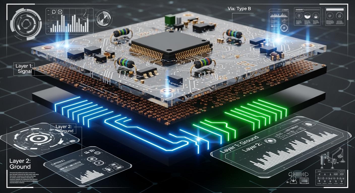
You need to know pcb stack-up design to make good boards. PCB stack-up is how you put layers in a board when you design it. This setup changes signal quality, EMI, and how easy it is to build the board. Picking the right materials and using stackup rules helps keep impedance steady and cuts down interference. Using a balanced stack-up and putting ground planes close to signal layers makes your board work better. Having power and ground layers helps protect signals and lowers EMI. If you use best practices, you stop mistakes and make strong designs as engineers.
Key Takeaways
Know why PCB stack-up design matters. It helps signal quality, cuts down interference, and makes building easier.
Put ground planes next to signal layers. This setup keeps signals strong and lowers electromagnetic interference (EMI).
Pick the best materials and thickness for your stack-up. This helps control impedance and makes sure your board works well.
Use good ways to arrange layers. Keep signal layers apart and make both sides even to stop problems.
Work with your fabricator early when you design. Their advice can help you not make expensive mistakes and make your board better.
PCB Stack-up Basics
Definition and Purpose
When you design a pcb, stack-up means how you put layers inside the board. These layers include signal layers, power planes, and ground planes stacked together. The stack-up is very important for how well your board works. It controls how signals move, how much noise or interference happens, and how easy it is to make the board.
You use pcb stackup design to handle many key jobs in your circuit. These jobs help your board work well and last long. The table below shows the main jobs a pcb stack-up does in your design:
Function | Description |
|---|---|
Makes sure signals travel without bouncing back or losing power, very important for fast signals. | |
Crosstalk Reduction | Places signal layers and ground planes to block interference between signals. |
Tests fast signals to find problems like bouncing and interference before making the board. | |
Thermal Management Innovations | Designs stack-ups to handle heat well, helping the device work better and last longer. |
Documentation | Keeps track of all layers as they grow, making sure every signal path is clear and recorded. |
By planning your stack-up carefully, you keep impedance steady. This stops signals from bouncing back and causing mistakes. You also lower crosstalk, which is when signals on one layer mess with others. Good stack-up design lets you test signal behavior before building the board. It also helps manage heat, keeping your board cool and working well. Lastly, clear stack-up documents help you and the maker understand the board’s details.
Types of Stack-ups
There are several common pcb stack-ups used in electronics. Each type fits different design needs, costs, and complexity. Here are the most usual stack-ups you will see:
2-layer PCBs
4-layer PCBs
Common 4-layer stack-ups include:
(SIG & PWR) / GND / GND / (SIG & PWR)
GND / (SIG & PWR) / (SIG & PWR) / GND
SIG / GND / PWR / SIG
Variations of 4-layer stack-ups:
SIG / GND / PWR / GND
GND / (SIG & PWR) / SIG / GND
GND / SIG / PWR / GND
In a 2-layer pcb stackup, you usually have one signal layer and one ground or power layer. This setup is good for simple boards or slow signals. When you use a multi-layer pcb stackup, like a 4-layer board, you get more control over signal quality and EMI. You can put power and ground layers close to signal layers, which makes the board work better.
More complex boards may have 6 or more layers. These boards let you separate signals, power, and ground into their own layers. This separation cuts down noise and crosstalk even more. It also helps control impedance and heat.
Choosing the right stack-up depends on your board’s job, signal speed, and budget. When learning pcb stackup design, start with simple layers and add more as needed. This way, you learn how each layer changes your board’s performance.
Tip: Always ask your PCB maker about their best stack-up choices. They can help you pick what works best for your design and making process.
Importance of PCB Stack-up Design
Signal Integrity and Performance
You must think about signal integrity when you plan your pcb stack-up. Signal integrity in dense pcbs depends on how you set up layers. It also depends on controlling impedance and picking good materials. High-speed signals move through the board. They can lose quality if you do not follow signal integrity rules. Keep signal layers close to ground planes. This setup helps keep signals strong and lowers noise. The table below shows how stack-up choices change signal integrity in high-speed pcbs:
Aspect | Description |
|---|---|
Layer Arrangement | Careful planning keeps signals strong and stops problems. |
Good control stops crosstalk and reflections. It keeps performance steady. | |
Material Selection | Good materials help with heat and make boards last longer. |
You meet signal integrity needs by using these stackup ideas. You protect signals and make sure your board works well.
EMI and EMC Considerations
You must think about emi/emc when you design for signal integrity. EMI means unwanted electromagnetic signals that can mess up your board. Bad stack-up can make high-speed traces send out interference. You can lower EMI by grounding, matching impedance, and using shielding. Signal integrity in dense pcbs gets better when you put ground planes near signal layers. An unbalanced stack-up, like putting many signal layers on one side without a ground plane, makes uneven return paths and raises EMI. A balanced stackup makes sure each signal layer has a reference plane. This shields your board and keeps signals strong.
Unshielded signal returns cause EMI problems.
Poor interplane capacitance lets emissions escape.
These problems are connected and need careful fixing.
Manufacturability Factors
You must think about manufacturability when you design your pcb stack-up. Complex stackups can be hard to make. Imbalances in layer symmetry and changes in dielectric thickness affect signal integrity in dense pcbs. Impedance mismatch can happen because copper etching is not always the same. Ground bounce can come from voltage changes on power planes. HDI boards need special lamination and drilling. Rigid-flex stack-ups need bonding different materials, which can cause delamination. You need detailed stack-up documents to stop mistakes and make sure you can repeat the process. Thermal cycling tests your board’s strength and reliability.
Tip: Always check your stackup documents before sending your board to be made. This step helps you find mistakes early and keeps your pcb design for signal integrity strong.
Layer Arrangement in PCB Stack-up
Layer Types and Functions
You should know the main types of layers in a pcb stack-up. Each layer has a special job on your board. Here is what each layer does:
Signal layers carry electrical signals between parts. They have traces, pads, and vias.
Power planes spread power across the pcb. They give a low-resistance path for voltage and current.
Ground planes reduce noise and give a common reference for signals. This helps signal quality.
Internal signal layers hold extra traces in dense pcbs. They help lower crosstalk and interference.
You use these layers to control signal quality and keep your board working well. High-speed signal layers need careful placing near a plane to keep signals clear.
Common Layer Configurations
You choose a stackup based on your design needs. The table below shows common pcb layer setups:
Layer Count | Description |
|---|---|
2-layer | Basic setup for simple uses. |
4-layer | Often used for a good mix of complexity and cost, fit for many devices. |
6-layer | Gives more routing space, great for complex designs. |
8-layer | Used for very dense designs needing lots of routing. |
You start with a simple board and add more layers as your design grows. More layers help you manage signal quality and make routing easier.
Power and Ground Planes
Power and ground planes are very important in your pcb stack-up. You put these planes next to signal layers to help signal quality.
Ground planes are key for keeping signal quality by giving a steady reference for signal return paths. This lowers breaks that can affect impedance control, which is very important at high frequencies. Also, ground planes help cut electromagnetic interference (EMI) by acting like shields, stopping emissions and blocking outside noise.
Good stack-up design gives signal traces the right reference planes and cuts signal loss.
Multiple ground planes reduce ground bounce and shield against EMI.
Ground planes improve electromagnetic compatibility by lowering emissions.
You keep your board steady by using power and ground planes in your stackup. This setup supports high-speed signals and keeps your design strong. Good plane placement helps you avoid noise and keeps signal quality high.
PCB Stackup Design Guidelines
Layer Assignment Rules
You should follow simple rules when you make a multi-layer pcb stackup. These rules help you build a good pcb stack-up that works well and lasts long. Here are some easy tips for picking layers in your pcb stackup design:
Put a ground plane next to every signal layer. This gives signals a safe path back and keeps them strong.
Route fast traces on inside layers between ground and power planes. This setup protects signals and lowers EMI.
Keep signal layers near their reference planes. This helps stop noise and keeps impedance steady.
Do not put two signal layers next to each other. This stops crosstalk and keeps your board neat.
Make your stack-up the same from top and bottom. Symmetry helps your board stay flat and strong.
Place power and ground planes close together. This raises capacitance and cuts down noise.
Leave enough space between power and ground planes. This helps your pcb stack-up work well and lowers EMI.
Use microstrips over thin dielectric material for fast signals. Thin dielectrics help control impedance.
Try to use fewer lamination steps. Fewer steps make your pcb stackup design easier and cheaper.
Tip: Always talk to your fabrication team about your stackup design needs. They can help you choose the best layer setup for your pcb stack-up.
Impedance Control
You need to control impedance in your pcb stackup design to keep signals strong. If impedance is not right, signals can bounce back or lose power, especially with fast signals. Here are some ways to keep impedance steady:
Use impedance calculators to guess impedance using stack-up, dielectric constant, and trace size.
Write down dielectric thickness and material details in your stackup design rules. This keeps impedance the same everywhere.
Put a solid ground plane under fast traces. This gives signals a safe path back and keeps impedance steady.
Add resistors at the ends of traces to match impedance and stop bouncing.
Match the impedance of pcb traces with the source and load. This keeps signals from getting weak on fast lines.
To control impedance in pcb stack-up design, you change trace width and thickness, pick the right dielectric, and set the distance to reference planes. You can use coplanar waveguide and differential pairs to get controlled impedance traces. These stack-up design rules help you lower EMI and keep your board working well.
Note: Work with your fabrication team to make a stackup that meets impedance needs. Good stackup documents help you avoid mistakes and make your pcb stack-up better.
Reducing Crosstalk and Noise
You need to lower crosstalk and noise in your multi-layer pcb stackup to keep signals clear. Crosstalk happens when signals on one layer mess with others. Here are some rules to help you lower crosstalk and noise:
Use controlled impedance traces for fast signals. This keeps signals clean and stops bouncing.
Put ground planes next to signal layers. Ground planes lower loop inductance and keep fields close.
Keep fast signal traces short and smooth. Short and smooth traces lower noise.
Leave enough space between traces. More space means less crosstalk and a stronger board.
Use resistors near the source or load to stop bouncing. These resistors help keep signals steady.
Use solid ground and power planes for low-inductance return paths. This lowers noise.
Do not split power planes unless needed. Splitting can mess up return paths and cause EMI.
Keep power and ground planes close together. Tight spacing raises capacitance and lowers noise.
Try to use fewer signal layer jumps. Fewer jumps mean fewer problems with return paths and EMI.
Put power and ground planes close to make a strong power network.
Split power planes for different voltages or sensitive analog parts.
Use copper pours on signal layers tied to power or ground. Copper pours make planes bigger and lower impedance.
Add lots of vias to connect power and ground planes. Vias lower plane impedance and help current flow.
Callout: Following pcb stackup design rules helps you avoid EMI, EMC, and impedance problems. You make a board that works well and keeps signals strong.
You can use these stack-up design rules to make a good pcb stack-up. Careful layer picking, impedance control, and noise cutting make your pcb stackup design strong and easy to build. You protect your board from EMI and keep signals clear by following these pcb stackup design rules.
Material Selection for PCB Stack-up
Dielectric Materials
You have to pick the right dielectric materials for your pcb stack-up. Dielectrics go between copper layers and help signals move through the board. FR-4 is the most used material for many pcb designs. It works for most boards and does not cost a lot. If you need high-speed or radio frequency designs, you might use Rogers or polyimide. These materials lose less signal and work better for fast signals. You should always look at the dielectric constant (Dk) and loss factor. These numbers show how well the material helps fast signals and keeps your stack-up strong.
Thickness and Properties
Dielectric thickness is important for how your pcb works. You need to choose the right thickness for your stack-up to get good results. Here are some ways thickness changes your board’s electrical performance:
Impedance control for signal integrity: The thickness of the dielectric changes impedance. You can pick a certain thickness to match your trace width and material for the right impedance.
Layer count and board thickness: If your pcb has more layers, you may need thinner dielectrics so the board does not get too thick.
Power plane capacitance: The thickness between power and ground layers changes capacitance. Thinner dielectrics give more capacitance and help filter noise. Thicker dielectrics are better for high-voltage designs.
You should always match dielectric thickness to what your design needs. This helps your stack-up support strong signals and keeps your board working well.
Cost vs. Performance
You need to think about cost and performance when you pick materials for your pcb stack-up. Some materials cost more but work better for high-speed or complex designs. The table below shows how different things affect your choices:
Factor | Description |
|---|---|
Signal Integrity | Low Dk materials help high-speed signals by lowering losses. |
Thermal Management | Good design choices help with heat and can save money. |
Manufacturability | Hybrid materials and even stack-up layers can lower manufacturing costs. |
Cost vs. Performance Trade | Expensive low Dk materials may let you use fewer layers and make routing easier. |
Design Strategies | Testing and simulation help you find the best mix of cost and performance for your board. |
You should talk to your fabricator about material choices for your stack-up. This helps you get good performance for your pcb without spending too much. Picking the right materials makes your board strong, reliable, and ready for your design goals.
Manufacturing Constraints in PCB Stackup Design
Minimum Layer Thickness
You must pay attention to the minimum layer thickness when you design a pcb stack-up. The thickness of each layer affects how well your board works and how easy it is to make. If you use layers that are too thin, your pcb can bend or break. If you use layers that are too thick, your board may not fit in your device. The table below shows a common minimum thickness for different pcb types:
PCB Type | Minimum Dielectric Thickness | Prepregs |
|---|---|---|
IPC Class 3 | 2.56 mil | 2 plies |
You should always check with your manufacturer to make sure your stack-up meets these limits. This helps you avoid problems during production.
Via Types and Placement
You need to choose the right via types and place them carefully in your stackup. Vias connect layers in your pcb and help signals move between them. Microvias can make your design more complex. They also affect how many times your board needs to be pressed together during manufacturing. Each layer where a microvia starts or stops adds a step to the process. This can make your pcb harder to build.
You should also think about the devices you use on your board. If you use ball grid arrays or parts with many pins, you may need more layers. The number of signal, power, and ground layers also changes how you design your stack-up. A good stackup reduces noise, crosstalk, and EMI. This makes your board more reliable.
Tip: Place vias away from sensitive signal paths. This helps you keep your signals clean and your board strong.
Stack-up Documentation
You must create clear stack-up documentation for your pcb. Good documents help your manufacturer build your board the right way. You should include the following details in your stackup documents:
Reference the general specification for printed circuit boards.
List all materials used in your stack-up drawing.
State the overall board thickness and allowed tolerance.
Show copper weight for each layer.
Give X and Y coordinates for all holes.
Set the minimum annular ring size.
Specify copper plating thickness for holes.
Describe the soldermask type and where to apply it.
Use nonconductive white ink for the legend.
Mark the board with supplier ID and date code.
Set the radius for inside corners and slots.
Do not change the film without approval.
Compare the CAD net list to the Gerber data before making the board.
Remove non-functional pads from inner layers.
Build conductor width and spacing to match Gerber data.
Follow all fabrication instructions for controlled cross-section boards.
Include a copy of the stackup sheet with the first delivery.
Allow thieving on outer layers for even plating.
Measure dielectric and copper thickness on one board from each lot.
Make sure drilled holes match CAD data closely.
Cap 12 mil vias from the BGA side with epoxy and soldermask.
You help your manufacturer avoid mistakes by giving clear stack-up documents. This step makes your pcb design process smoother and your board more reliable.
Thermal Management in PCB Stack-up
Heat Dissipation Techniques
You need to control heat in your pcb stack-up. Heat builds up when parts run for a long time. High-power devices also make boards hotter. You can use different ways to spread heat and keep your board cool:
Ground planes are big surfaces that soak up heat. They spread heat across the board. Ground planes also give signals a safe path.
Copper pours fill empty spaces and move heat away from hot spots. Heavy copper pours add more mass. This slows down fast changes in temperature.
Thermal vias are holes filled with copper. They connect layers and lower thermal resistance. Copper-filled vias work better than air-filled ones.
Heavy copper layers make more space for heat to flow. This helps ground planes act as heat sinks.
Embedded copper coins give a metal path for extreme heat. You use these coins for parts that get very hot.
You can use more than one method in your stack-up. Good choices help your pcb last longer and work better.
Tip: Put thermal vias close to hot parts. This helps heat move fast from the surface to inside layers.
Material Choices for Thermal Performance
You need to pick good materials for your pcb stack-up. Each material changes how your board handles heat and temperature. The table below shows common materials and how they affect heat:
Material Type | Description | Thermal Properties Impact |
|---|---|---|
Substrate Materials | Materials like FR-4 and polyimide give support. | Picking the right one helps your board resist heat and work well. |
Copper Foils | Layers that carry signals. | Thicker foils lower resistance and help spread heat. |
Prepregs | Layers that hold the board together. | The material changes both electrical and heat properties. |
Core materials like FR-4 make your board strong and safe. For high-frequency designs, you might use Rogers RO4350B. It loses less signal and handles heat better. Copper foils help spread heat. Thick foils move heat away from hot spots. Prepregs keep layers together and change how your board deals with heat.
You should match materials to what your design needs. This helps your pcb stack-up handle heat and keeps your board safe while it works.
Best Practices for PCB Stack-up Design
Avoiding Common Pitfalls
You can stop many problems in pcb stackup design by learning from common errors. New engineers often face issues that hurt board performance and reliability. The table below shows common mistakes and how they affect your pcb:
Pitfall | Description |
|---|---|
Imbalances in layer symmetry | Cause signal problems because electrical properties are uneven. |
Dielectric thickness variations | Lead to impedance mismatches and signal reflections. |
Inadequate plane allocation | Create ground bounce and EMI, which lower board reliability. |
Missing reference planes | Make stack-ups unbalanced and hurt high-speed signal quality. |
Happen when dielectric details are missing, causing design errors. |
Also, watch out for these errors in your stackup:
Setting impedance without full dielectric info.
Using an unbalanced stack-up.
Leaving out reference planes under fast signal layers.
Not matching copper weights with impedance goals.
Picking dielectric thickness that breaks via aspect ratio rules.
Calculating impedance and trace width with wrong dielectric thickness.
Forgetting to set fabrication limits for thickness, trace width, or impedance.
Putting surface finish and solder mask layers in the wrong order.
You can avoid these problems by checking your stackup design twice. Keep clear records for every board you make.
Collaboration with Fabricators
You make pcb stackup design better by working closely with your fabricator. Good communication helps you learn about the making process and materials in your stack-up. Always share your stackup plans early and ask for feedback. This helps you meet limits like controlled impedance, crosstalk, and interplane capacitance.
Working with your fabricator gives you these benefits:
You make sure your pcb meets making and quality rules.
You cut errors by giving detailed stack-up documents.
You keep production the same for all boards.
You check drilling accuracy and alignment, which matter for signal quality.
You get advice on best ways to design a high-density multi-layer stackup.
Treat your fabricator as a partner in your design work. This teamwork leads to better pcb stack-up results for simple and complex projects.
Tip: Always review your stackup with your fabricator before finishing your board design. This step saves time and stops costly mistakes.
Sample PCB Stack-up Examples
2-Layer Stack-up
You usually start with a 2-layer pcb when learning stackup design. This board is simple and good for basic circuits. There are two copper layers with a core in the middle. The top and bottom layers carry signals or power. The core keeps them apart. You use vias to connect both sides. In a normal 2-layer stack-up, you see:
Signal layer: The top copper layer is about 0.0014 to 0.0021 inches thick.
Laminate core: This layer sits between copper layers and supports the board.
Bottom layer: The bottom copper layer is also about 0.0014 to 0.0021 inches thick.
This stack-up is used for cheap and easy designs. It helps you learn stackup basics before using more layers.
4-Layer Stack-up
A 4-layer pcb stack-up gives you more control over signals and noise. You see this board in many hobby and simple projects. It has four conductive layers with insulation between them. The most common stack-up has a top signal layer, a ground plane, a power plane, and a bottom signal layer. This setup makes signals better and lowers noise. It also gives better power and more ways to route traces.
Feature | Description |
|---|---|
Structure | Four conductive layers separated by insulating materials. Typical: Top signal, Ground, Power, Bottom signal. |
Advantages | Better signals, less noise, improved power, stronger EMI/RFI shielding, more routing choices. |
Common Applications | Used in computer motherboards, telecom gear, industrial systems, medical devices, cars, and high-end audio. |
When to Choose | Pick this when your design is complex, needs fast signals, or needs strong signal quality and EMI/RFI shielding. |
You pick a 4-layer stack-up when your pcb needs more performance than a 2-layer board.
6-Layer Stack-up
A 6-layer pcb stack-up gives you even more options and performance. You use this stack-up for advanced designs. It adds extra signal and plane layers. These help with routing and signal quality. You get better EMI shielding and heat control. The table below shows how a 6-layer stack-up compares to a 4-layer stack-up:
Aspect | 6-Layer Stack-Up | 4-Layer Stack-Up |
|---|---|---|
Routing Flexibility | More signal layers make routing easier | Fewer ways to route |
Signal Integrity | Better for high-speed designs | Good for normal speeds |
EMI Shielding | More ground planes for stronger EMI | Basic shielding |
Thermal Management | More copper area for heat control | Less heat control |
Cost | Higher because it is more complex | Lower cost |
Design Complexity | Needs more planning and design work | Easier process |
You choose a 6-layer stack-up when your board needs fast signals, strong EMI control, and better heat handling. This stack-up fits advanced electronics and tough projects.
To make a strong pcb stack-up, you need to follow some steps. Use ground planes because they help cut down noise. Put high-speed signals on inside layers to keep them safe. Keep signal layers close to ground layers for better results. Make sure your board is even on both sides. Pick the right materials and dielectric thickness to control impedance. If you follow pcb stack-up design rules, your signals stay clear. You also get less EMI and your board is easier to make. Always work with your fabricator so your board can be made right and you do not waste money. Keep learning by reading trusted guides to get better at pcb stack-up and make great pcbs.
Resource Title
Link
PCB Stackup Design Guidelines for Performance With OrCAD X
https://resources.pcb.cadence.com/blog/2023-pcb-stackup-design-considerations
PCB Stack-up Design Rules
PCB Stackup Optimization: Engineering Robust Electronics
Comparison of PCB Material Properties for High Speed Design and HDI Boards
https://resources.altium.com/p/materials-for-high-density-interconnects
Enhancing Signal Integrity in PCB Design: Key Considerations and Strategies
FAQ
What is the main purpose of a pcb stack-up?
You use a pcb stack-up to organize the layers in your board. This setup helps you control signal quality, reduce noise, and make your board easier to manufacture.
How do power and ground planes help my design?
Power and ground planes give your signals a steady path. They lower noise and help protect your board from interference.
Why should I talk to my fabricator before finalizing my design?
Your fabricator knows the best materials and processes. You get advice that helps you avoid mistakes and makes sure your board meets all requirements.
Can I use the same stack-up for every project?
You should not use the same stack-up for every project. Each design has different needs. You must match your stack-up to your board’s speed, size, and function.
What happens if I ignore impedance control?
If you ignore impedance control, your signals can bounce or lose strength. This can cause errors and make your board unreliable.
See Also
Investigating Common Stack-up Configurations for HDI PCBs
Essential Skills for Designing Multi-layer PCB Layouts
Evaluating Costs and Benefits of Advanced HDI PCB Designs
Frequent Challenges and Solutions in PCB SMT Design
Challenges in Manufacturing and Prototyping Multi-layer PCBs
