Common Stackup Mistakes & 7 Proven Design Fixes for PCB Warpage
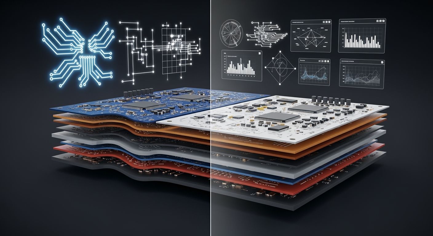
IPC rules define bow as a curved shape where all four corners remain flat. IPC-TM-650 2.4.22 defines twist as diagonal corner bending. Uneven layer designs and unequal copper weight cause severe heat bending during circuit board soldering. You can manage board bending by setting strict factory limits.
IPC Class | Application Type | Max Bow/Twist (%) |
|---|---|---|
Class 2 | SMT (industrial) | 0.75% |
Class 3 | SMT (high-reliability) | 0.50% |
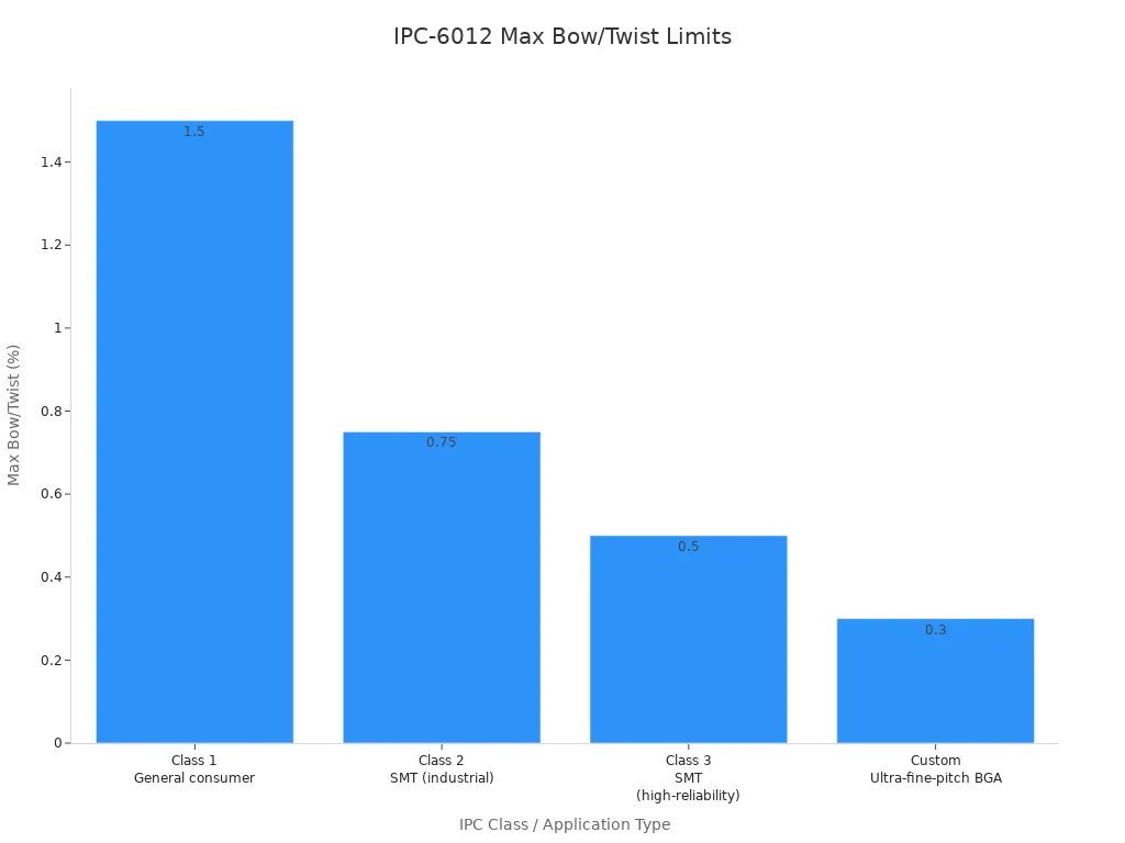
IPC-6012 sets acceptable limits at 0.75% for regular SMT and 0.50% for fine-pitch BGA. You protect every circuit board by Avoiding PCB Warpage with uniform pcb warpage limits.
Key Takeaways
Uneven circuit layers and unbalanced copper make the board bend during hot soldering.
Mirrored layer designs keep material thickness and copper weights equal across the center line.
Copper thieving balances metal thickness and stops the board from shrinking unevenly.
High-Tg laminates resist damage from heat and keep circuit boards flat inside reflow ovens.
Baking PCB materials early unlocks trapped inner stress and clears out dangerous hidden moisture.
Understanding PCB Warpage and Thermal Mechanics
Coefficient of Thermal Expansion and Thermal Stress
Heating temperatures from 245°C to 260°C trigger strong physical expansion inside board fabrications during assembly reflow. Copper foil expands evenly at 17 ppm/°C in all directions. Standard FR4 laminate expands at 14-17 ppm/°C along the XY axis, while its Z-axis expansion jumps to 50-70 ppm/°C. This huge CTE mismatch across material borders creates internal bending forces that cause pcb warpage.
Irreversible size changes in FR4 PCBs during the first heating after making come mostly from post-curing and lingering stress inside the FR4 laminate structure.
Flexible polymer behavior traps lingering stress in the resin matrix during ongoing crosslinking. When high heat hits unbalanced copper layers, copper-heavy layers shrink less than copper-light layers as they cool down. This uneven shrinking pulls structural materials out of line, which ruins the flatness of the board.
Bow vs Twist Mechanical Differences
Mechanical stress changes the physical shape of a board through two clear geometric distortions. Observing how the corners lie on a flat surface helps you tell these deformations apart easily.
Deformation Type | Shape Characteristics | Surface Boundary Condition |
|---|---|---|
Bow | Cylindrical or spherical curve along one axis | All four corners stay in the same plane |
Twist | Twisted distortion along the diagonal axis | Three corners touch while the fourth corner lifts |
IPC standards describe bow as a cylindrical bending shape where all four corners stay on one flat plane. Unbalanced axial forces cause this smooth curve across the length or width of the board.
Conversely, twist creates diagonal corner warping where the corners fail to stay on the same flat surface. IPC-TM-650 Method 2.4.22C calculates this distortion with the formula Twist % = (TwistDist / (2 × DBoard)) × 100%. You measure TwistDist as the height gap while pressing two opposite corners onto a flat reference table. Stopping this twist-induced warpage requires balancing copper density and material features throughout your stackup.
Common Stackup Errors and Avoiding PCB Warpage
Asymmetrical Layer Construction
Unequal layer stackups create uneven internal forces and bad bending during factory heat-pressing. You make heat strain when you mix different prepreg types or different core insulator thicknesses across the middle line. Makers lose good boards when mismatched materials create permanent stress through the inner layers. Thin high-density connection insulators around 50 µm to 75 µm pass this shape mismatch much faster than standard stiff cores.
Unbalanced insulation layers cause expected bending during hot baking cycles. Unequal plastic distribution forces thicker insulation spots to shrink more when the board cools off. This uneven shrinking pulls your board build toward the thinner side, causing shape damage and diagonal twisting. Makers often ask for layer changes when unequal insulation gaps make pressing steps harder. You must copy all prepreg types and insulation thicknesses across the center line for avoiding pcb warpage.
Uneven Copper Weight Distribution
Unequal copper weight layout between layers causes uneven growing under hot solder heat. Heavy power layers on one side compared to thin signal layers on the other side cause constant inner stress. Copper-heavy layers grow much more during heat steps, making a potato chip bend shape across your board setup. Repeated heat changes make these inner stresses build up over time. Matching copper amounts between copy layer pairs directly balances heat-caused stress and helps in avoiding pcb warpage.
Big copper-amount differences over 30% across a layer pair cause local physical strain. Copper grows about four times faster than standard board base material. This growth gap creates pcb warpage because heat cycles push the board to bend toward the lighter copper side. You save signal strength and keep panel flatness by placing fake copper fills in empty spots. Adding balance grids stops local bending near sensitive parts and cuts bending across all inside layers. Copying heavy power layers stays key for avoiding pcb warpage, while early factory checks protect your board against pcb warpage.
7 Proven Design Fixes to Prevent Board Warpage
Engineers make smart layout adjustments to stop board warpage during hot reflow soldering. Circuit board materials swell unevenly along the Z-axis while heating up. Temperature differences across uneven layers create strong inner bending forces. You can remove these internal forces by matching material properties and balancing copper around the center line. Using clear layout rules keeps your circuit board safe from permanent heat damage.
Design Symmetrical Mirror Stackups
You must build mirrored layer arrangements around the center of the board for avoiding pcb warpage. Using identical insulation thickness, resin content, and material traits keeps mechanical forces equal on both sides during reflow. For example, a balanced 6-layer HDI board using 0.305 mm cores on top and bottom keeps shape changes under 0.75%. However, an unbalanced board mixing a 1.5 mm core with a 0.305 mm core creates 1.5% or worse bending.
Design Aspect | Mirrored Stackup Rule |
|---|---|
Dielectric thickness | Identical on both sides of the central plane, such as matching a 0.2 mm dielectric between layers 1–2 with a 0.2 mm dielectric between layers 7–8. |
Dielectric material | Same material properties on both sides, such as FR-4 with a dielectric constant of 4.2–4.5. |
Core and prepreg uniformity | Uniform core and prepreg thickness across paired layers to avoid lamination stress. |
Matching the coefficient of thermal expansion values for core and prepreg layers across all sides is also necessary. Using equal material stiffness across opposing insulation layers stops physical bowing as the board cools. Furthermore, putting the same copper weights on paired layers prevents uneven physical strain. You should also design matching part land patterns under every surface connection point. Equal pad shapes balance local pull forces across the board surface during hot soldering steps.
Balance Copper Density and Utilize Thieving
Unequal copper spacing creates strong physical strain across metal layers during hot manufacturing steps. You get even copper coverage by adding extra copper patterns inside empty signal areas.
Adding copper thieving to sparse inner layers balances copper density, controls resin flow during lamination, and stabilizes the board during heating.
You must place hatched copper fills or extra metal in blank spaces while leaving 0.5 mm space from fast signals to protect signal quality. On power planes, cross-hatched copper fills balance material layout without causing bad heat expansion problems. Setting hatch spacing to about 25–50% copper coverage easily balances thermal expansion. Specifically, using a 50% hatch pattern balances heat expansion between layers while keeping signals clean.
Finally, adjust total panel sizes and edge rail setups to strengthen the entire manufacturing array. Building balanced edge rails protects every single board from twisting diagonally during cutting steps. Adding extra copper to waste rails spreads heat evenly across the whole panel assembly.
Following these structural rules helps you in avoiding pcb warpage across big factory runs. Clear physical design rules help control every board warpage limit. Fixing board warpage early stops expensive factory delays. Good balance stops board warpage on complex boards. Keeping expansion equal prevents board warpage under heat.
Material Selection for Preventing PCB Warpage
High-Tg and Low-CTE Laminate Selection
Picking strong core and prepreg materials forms your main defense against pcb warpage. Normal FR4 laminates feature a low glass transition temperature near 130°C to 140°C. These basic base materials soften quickly inside lead-free solder ovens because their Z-axis coefficient of thermal expansion jumps from 60–70 ppm/°C below Tg up to 250–300 ppm/°C above Tg. You can choose high-Tg laminates with ratings at or above 170°C, like ITEQ IT-180A or IS410 at 180°C. High-Tg materials hold physical strength across tough heating steps, directly lowering pcb warpage risk during building.
Material Type | Glass Transition Temp (Tg) | Z-Axis CTE (Below Tg) | Z-Axis CTE (Above Tg) | Thermal Stress Effect |
|---|---|---|---|---|
Standard FR4 | 130–140°C | 60–70 ppm/°C | 250–300 ppm/°C | Softens near reflow, increasing deformation risk. |
High-Tg FR4 | 170–180°C | 45–55 ppm/°C | 200–250 ppm/°C | Retains mechanical rigidity and lowers stress. |
High-Tg options keep your board flat under strong solder heat. Lower Z-axis expansion reduces physical gaps between conductive copper foils, glass fibers, and component pads. This better shape control stops heat-made warpage across complex multilayer stackups and heavy copper designs.
Pre-Baking Laminates Above Glass Transition Temperature
Baking laminates near or above their glass transition temperature relieves lingering stress and reduces warpage during thermal reflow exposure.
You remove built-up physical strain by pre-baking board laminates before part attachment. Regular panel building locks internal stress inside plastic layers during high-pressure pressing steps. Controlled baking cycles let linked plastic chains settle into place for good. This heat treatment balances board shape, so your factory run fights diagonal twisting and bad pcb warpage during hot solder passes.
Clearing out trapped air moisture with pre-baking stops dangerous internal steam bubbles. Sudden water boiling during soldering creates board layer splits, surface bubbles, and fast warpage. Baking raw materials softens inner plastic parts and safely releases built-up physical strain. Makers get steady flatness across tricky designs, greatly improving overall warpage control.
Measuring and Validating Board Warpage Limits
Applying the IPC-6012 Warpage Formula
Engineers check bending limits by using the standard IPC-TM-650 2.4.22 test steps. Official IPC-6012 rules list the maximum allowed bending numbers for finished circuit boards. You figure out the highest allowed bow along a board using RL = L × B / 100. In this math, L is the length in millimeters and B is the set bow percentage. Surface-mount parts need a tight 0.75% limit, while simpler designs can use up to 1.5%.
You figure out the highest allowed twist with the math rule R = 2 × D × T / 100. Here, D is the diagonal length in millimeters and T is the set twist percentage.
Case | Bow limit side 300 mm | Bow limit side 200 mm | Twist gauge size R |
|---|---|---|---|
Panel without SMD (B/T = 1.5%) | 300 × 1.5 / 100 = 4.5 mm | 200 × 1.5 / 100 = 3.0 mm | 2 × 360.56 × 1.5 / 100 = 10.82 mm |
Panel with SMD (B/T = 0.75%) | 300 × 0.75 / 100 = 2.25 mm | 200 × 0.75 / 100 = 1.5 mm | 2 × 360.56 × 0.75 / 100 = 5.41 mm |
A board measuring 200 mm by 300 mm has a diagonal line of 360.56 mm. Any corner gap larger than 5.41 mm fails the safety test.
Production Floor Measurement Techniques
Factory workers use several basic tools to check for curved or twisted boards. Simple pin tools offer a fast way to test basic board shapes. Even so, hand-held flat gauges can still skip over tiny surface bends.
Modern factory floors use smart light meters and high-tech laser scanners instead. These automatic tools collect complete surface height numbers very quickly across detailed panels.
Method type | Examples | Role in IPC-6012 validation |
|---|---|---|
Visual/manual | Mechanical gauges | Quick screening; may miss small curves |
Contact measurement | Feeler gauges, CMMs | Touches panel; can be slower |
Non-contact measurement | Laser scanners | Full-field, fast, precise measurement |
Procedure | IPC-TM-650 2.4.22 | Defines bow and twist steps |
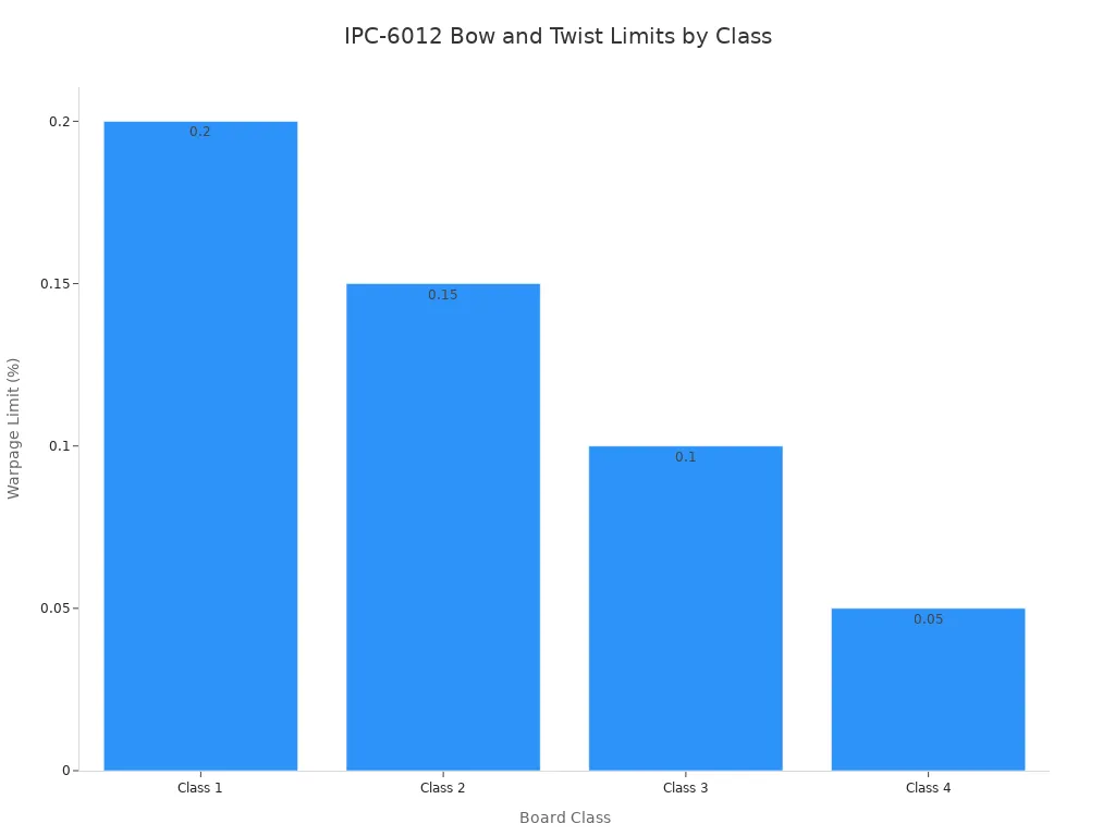
Limits | Class 1: 0.2%; Class 2: 0.15%; Class 3: 0.1%; Class 4: 0.05% | Pass/fail thresholds for validation |
Using light sensors keeps human testing mistakes from ruining the final results. Running early laser scans spots pcb warpage quickly and stops broad board warpage before putting parts on the board.
Unbalanced layer setups and uneven copper weight cause bad bending during hot assembly. Mixing different insulating materials or drawing uneven power layers around the middle line creates strong internal stress. Placing copper evenly and matching center materials early in your design phase stops heat damage during high-temp building.
You can stop pcb warpage by using equal insulation thickness and placing extra copper fills. Checking layer balance early removes bending hazards before full factory runs start. Work with your maker to run automatic layer and heat balance checks before sending final Gerber files so you can fix pcb warpage, control bending, and keep every board completely flat.
FAQ
What IPC standard defines acceptable board warpage limits?
IPC-6012 gives clear limits for how much a board can bend. Basic surface-mount parts allow a highest bend of 0.75%. Tiny-pin BGA parts need a lower boundary of 0.50%. Checking these numbers during testing stops building problems later.
How does symmetrical stackup design prevent warpage?
Matching layer designs keeps physical push forces equal across the middle of your board. You copy center cores, soft layers, and metal weights on both sides. This equal setup stops heat strain during baking, directly lowering bending risks.
Why does low copper density cause board warpage during reflow?
Unequal metal placement causes uneven heat growth across different board layers. Metal grows much faster than base plastic. Areas with less metal shrink more while cooling down, pulling the base off balance. Putting extra metal patterns balances this heat strain to stop bad bending.
Which laminate properties best protect against board warpage?
Strong base sheets give the best protection against high heat damage. You should pick materials that stay firm above 170°C. These solid sheets keep their shape and show lower thickness growth, stopping board bending inside hot baking ovens.
See Also
Solving Frequent Circuit Board Design Issues In Modern SMT Assembly
Understanding The Most Common Layer Stackups For HDI Multilayer Boards
Seven Vital Quality Control Steps For Automotive Heavy Copper Assembly
Essential Safety Guidelines And Tips For Successful Circuit Board Layouts
Key Principles You Must Master For Advanced Multilayer Board Design
