High-Layer Count PCB Manufacturing Process Challenges

You face hard problems when you work with high-layer-count pcb designs. Things like layer alignment, via reliability, and signal integrity can cause mistakes. These mistakes can break signal paths or even make short circuits. These problems make the PCB Manufacturing Process harder and cost more than normal boards. The table below shows how these problems change reliability, cost, and performance:
Challenge | Impact |
|---|---|
Layer Alignment Issues | Mistakes, bad signal integrity, and less function |
Via Reliability Problems | Problems in signal and power transmission |
Signal Integrity Concerns | Loss of performance, especially in fast designs |
Increased Manufacturing Costs | More money spent because of better technology and testing |
Knowing about these problems helps you make stronger and better projects.
Key Takeaways
High-layer-count PCBs have special problems. These include layer alignment, via reliability, and signal integrity. Knowing about these problems helps make design and manufacturing better.
Good layer alignment is very important. Even small mistakes can cause big signal problems. Always check alignment at every step in making the board.
Vias need to work well for signals and power to move right. Keep aspect ratios low to stop plating and heat issues.
Signal integrity is key for good performance. Use controlled impedance and low-loss materials to keep signals strong. This is extra important for high-speed uses.
Design and manufacturing teams should work together early. This can lower costs and make boards better. Use design for manufacturability (DFM) rules to make production easier.
High-Layer-Count PCB Overview
Definition and Applications
High-layer-count pcb boards are used in advanced electronics. These boards have more than twelve layers stacked on top of each other. Each layer moves signals or power. You use these boards when circuits are complicated and space is small. High-layer-count pcb boards let you fit many connections in a tiny area.
You can find high-layer-count pcb boards in important areas:
Telecommunications: Telecom server boards use high-layer-count pcb boards. Some boards have up to 24 layers. These boards move data quickly and connect many things.
Automotive: Modern cars use high-layer-count pcb boards. They help with safety and control by holding many circuits close together.
Medical devices: Medical equipment needs high-layer-count pcb boards. These boards help with tricky jobs and careful measurements.
High-layer-count pcb boards give you more options and power. You can make devices that are faster and smarter.
Unique Manufacturing Challenges
Making high-layer-count pcb boards is harder than making regular boards. You need to be careful at every step.
Layer alignment issues: Every layer must be in the right spot. Even small mistakes can cause big trouble.
Via reliability problems: Vias connect the layers together. If vias do not work, signals or power can stop.
Signal integrity concerns: Signals must be kept safe from noise. Fast signals need special design on these boards.
Poor plating quality: Sometimes the metal layers have problems. These problems can make the board weak.
Thermal stress and delamination: You must watch the heat during making. Too much heat can make layers come apart.
Stricter design and manufacturing practices: You must follow tighter rules to make sure the boards work well.
You need to know about these problems. High-layer-count pcb boards need more skill and care than regular boards. You must use the best ways to get good results.
Key Challenges in PCB Manufacturing Process
When you make high-layer-count PCBs, you face special problems. These problems make building harder than making regular boards. Every step can cause issues that change the final board. The table below shows main steps and their challenges:
Process Step | Unique Challenges |
|---|---|
Lamination | Needs high heat and pressure; mistakes can cause big errors. |
Alignment | Layers must line up exactly; small shifts can break signals. |
Drilling | Wrong drill spots can cut traces or make shorts. |
Plating | Vias must connect well for good board performance. |
Layer Alignment and Registration
Layer alignment is a big problem in pcb manufacturing. You stack many layers on top of each other. If layers are not lined up, signals can break or short. Even tiny moves can cause big problems. High-layer-count boards need tighter control than regular boards. You must keep registration within ±50 μm. Standard boards allow ±75 μm. If you miss this, vias, traces, and pads do not match. This hurts signal integrity and causes defects.
Tip: Check alignment at every step. Small mistakes get worse with more layers.
Via Reliability and Aspect Ratio
Vias connect layers in your pcb. High-layer-count boards use more vias. These vias must work well. Aspect ratio is the depth divided by width of the via. If aspect ratio is too high, plating and heat problems can happen. For drilled through-hole vias, keep aspect ratio at 10:1 or less. Higher ratios can cause bad plating and cracks. Laser-drilled microvias work best at 1:1 ratio. Picking the right via size stops defects and keeps boards strong.
High aspect ratios can make plating thin or uneven.
Large ratios can make vias fail when boards heat or cool.
Bigger drill sizes lower aspect ratio and help reliability.
Signal Integrity Issues
Signal integrity gets harder with more layers. You must keep signals clean and free from noise. High-layer-count boards have more crosstalk and EMI. This happens because traces are closer and there are more layers. You also see more signal loss, especially at high speeds. Using standard materials like FR-4 can lose more signal. You need good spacing, ground planes, and low-loss materials to keep signals strong.
Issue | Description | Causes | Solutions |
|---|---|---|---|
Crosstalk and EMI | Interference from nearby traces or layers, especially in dense designs. | Not enough space, bad grounding, impedance mismatches. | Make traces farther apart, use guard traces, add ground planes, check impedance. |
Signal Loss and Attenuation | Worse because of long traces and losses at high frequencies. | Using FR-4, long vias or traces, skin effect at high frequencies. | Use low-loss materials, make vias shorter, change trace width and copper thickness. |
Delamination and Pressing Difficulties
You press all layers together in pcb manufacturing. Too much heat or pressure can cause delamination. This means layers come apart and cause defects. High-layer-count boards need careful pressing. You must control heat and pressure closely. If not, you get bubbles, weak spots, or layers separating. Delamination ruins boards and wastes time and money.
Reflow and Soldering Defects
When you solder parts onto your pcb, you must heat the board evenly. High-layer-count boards have more thermal mass. Some areas heat or cool at different speeds. This can cause defects like tombstoning, where one end lifts up, or cold solder joints, which break easily. You can also see solder voids, poor wetting, and board warping. You must watch placement and heating to stop these problems.
Solder Voids: Air pockets block heat transfer.
Insufficient Wetting: Weak joints from dirty pads or bad flux.
Tombstoning: One end stands up, breaking the connection.
Cold Solder: Joints crack under stress.
PCB Warpage: Board bends and parts do not line up.
Increased Cost and Fabrication Time
Making high-layer-count boards costs more than regular boards. Each extra layer adds time and money. You need better materials, more tests, and tighter controls. The chart below shows how costs go up with more layers:
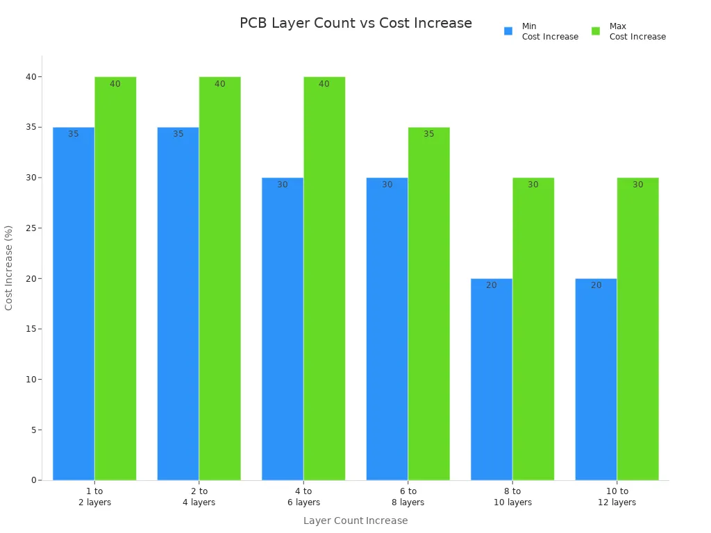
Going from 4 to 6 layers can raise costs by up to 40%. Lead times also get longer, often 14 to 21 days for high-layer-count boards. You must plan for extra costs and time before starting your project.
Note: High-layer-count PCBs need more skill, better tools, and more time than regular boards. You must get ready for these problems to avoid delays and extra costs.
Causes and Effects of High-Layer-Count PCB Challenges
Root Causes of Alignment and Registration Errors
You need to make sure each layer lines up right. Even tiny mistakes can cause big trouble. Layers can move because materials shrink or heat changes. If pressure is not even, layers can slip. Tooling holes that are not exact make things worse. Handling the panels badly can also mess up alignment. The table below shows what causes problems and what happens:
Root Cause | Manufacturing Impact |
|---|---|
Inner layer material shrinkage | Dimensional variation |
Lamination pressure imbalance | Layer slippage |
Temperature inconsistency | Differential expansion |
Inaccurate tooling holes | Registration deviation |
Poor panel handling | Cumulative alignment error |
Impact of Via Failures and Aspect Ratio
Vias link the layers in your pcb. If the aspect ratio is too high, you get problems. Plating can be weak and make the board less strong. Heat can crack vias and break the board. Bad vias can mess up signals and cause mismatches. You should pick the right via size and keep aspect ratios low.
Sources of Signal Integrity Problems
Signal integrity problems happen when traces are too close. Bad grounding can also cause trouble. When layers are packed tight, crosstalk and interference go up. Using regular materials can make signals weaker. You need to space traces out, use ground planes, and pick better materials.
Causes of Delamination and Pressing Issues
Delamination means layers pull apart during making. Bad resin bonding can make layers not stick. If materials do not match, they may not bond well. Too much heat can stress the board and break the glue. Water inside the board can turn to steam and push layers apart. Wrong heat or pressure during lamination can also cause problems. The table below lists what can go wrong:
Factor | Description |
|---|---|
Poor resin bonding | Not enough stick between layers can make them separate. |
Material incompatibility | Different materials may not join well and cause delamination. |
Thermal stress | Too much heat can make the glue too weak. |
Moisture absorption | Water inside can turn to steam and push layers apart. |
Improper lamination params | Wrong heat or pressure can cause layers to come apart. |
Effects of Uneven Heating and Soldering Defects
If the board heats unevenly, soldering can go wrong. Tombstoning happens when one end of a chip lifts up. Cold joints form if the solder does not melt all the way. Water inside can turn to steam and cause layers to split. You can stop these problems by drying boards, using the same solder paste, and keeping heat steady.
Cost Drivers in Complex PCB Manufacturing
Many things make high-layer-count pcbs cost more:
Cost Driver | Description |
|---|---|
Non-Standard Layer Counts or HDI | Special materials and tricky routing cost more. |
Design Phase Activities | Engineering work and paperwork add to costs. |
PCB Fabrication | More layers, drill types, and finishes raise the price. |
Production Volume | Small batches cost more per board, big orders cost less. |
Testing Requirements | Extra testing costs more, especially for fast signals. |
Special materials, more work, and extra tests all make the price go up. You should plan for these costs before you start your project.
Solutions and Best Practices for PCB Manufacturing
Advanced Layer Registration Methods
You can make multilayer pcb alignment better with special methods. Laser direct imaging helps you keep patterns sharp. X/Y scaling compensation stops layers from shrinking too much. Storing materials the right way keeps their size steady. Multi-stage pressing and pin registration help layers stay in place. High-precision drilling uses CNC machines and X-ray checks to put holes in the right spots. After pressing, X-ray and SPC tracking check if layers are lined up well.
Method | Control Method | Accuracy Benefit |
|---|---|---|
Inner Layer Imaging & Scaling | LDI exposure, X/Y compensation | High pattern precision, shrinkage control |
Material Behavior Management | Characterization, storage | Predictable alignment, stable dimensions |
Lamination Process Optimization | Multi-stage, pin registration | Reduced layer shift, repeatability |
High-Precision Drilling | CNC, X-ray alignment | Precise hole placement, via registration |
Post-Lamination Inspection | X-ray, SPC tracking | Verify alignment, continuous improvement |
Enhancing Via Reliability
You can make vias stronger by using good process controls. Drilling with the right speed makes holes clean. Plasma and wet desmear clean the hole surfaces well. Thick copper plating and pulse plating make vias last longer. Testing with coupons and AOI finds problems early. Microsection analysis checks if the process is stable.
Process Control | Description |
|---|---|
Optimized drilling | Enhances hole quality, reduces defects |
Desmear optimization | Improves via surface |
Thick copper plating | Increases connection reliability |
Pulse plating | Improves plating quality |
AOI/testing | Isolates defects, validates process |
Improving Signal Integrity
You can keep signals strong by stacking layers the right way. Controlled impedance helps high-speed signals stay safe. Using advanced laminates stops signal loss. Keep high-speed traces apart to lower crosstalk. Route pairs with equal length and spacing. Simulate and test your board to check performance.
Stack layers for good signal integrity.
Use controlled impedance for fast signals.
Pick materials that stop signal loss.
Keep traces apart to reduce crosstalk.
Test and simulate your board design.
Preventing Delamination and Pressing Failures
You can stop delamination by storing materials where humidity is low. Use laminates with low CTE for better strength. Press layers with even pressure to avoid weak spots. Vacuum lamination removes air bubbles. Match prepreg and core materials to your needs. Watch temperature, pressure, and vacuum closely. Test after pressing to check for problems.
Tip: Always look for bubbles and weak spots after pressing.
Managing Reflow and Soldering Quality
You can make soldering better by using thermocouples for heat checks. Make virtual reflow profiles based on your board. Measure heat in real time and check solder joints. Simulate how boards will be made and test for reliability. Change profiles if needed and let boards cool between runs.
Reducing Cost and Lead Time
You can save money and time by making drilling simpler. Use panels well to get more boards from each batch. Pick surface finishes that fit your needs and supply chain. Use design for manufacturing to lower layer counts. Make board shapes and panels work best in fabrication. Choose materials with the right Tg and copper weight.
Note: Working together early and testing a lot helps you get better boards and higher yield in high-density designs.
Preventive Measures and Collaboration in PCB Projects
Early Design-Manufacturing Collaboration
You can make high-layer-count pcb projects better by working together early. If design and manufacturing teams talk at the start, they find problems sooner. This teamwork stops big mistakes and helps the project go well. The table below shows how early teamwork helps your project:
Benefit | Description |
|---|---|
Reduced Respins | Early DFM input helps find design problems before making boards, so you do not need to redo work. |
Increased Yield | Working together makes designs fit the building process, so more boards turn out right. |
Lower Total Cost | Fixing problems early saves money for the whole project. |
Tip: Talk to your manufacturer when you start your design. This step saves both time and money.
Applying DFM Guidelines
You should always use design for manufacturability rules. These rules help you make boards that are easier to build and work better. For high-layer-count boards, some rules are extra important. The table below lists the top rules to follow:
Guideline | Description |
|---|---|
Trace Width and Spacing Optimisation | Use at least 6 mils for trace width and space to stop shorts or over-etching. |
Use of Standard Component Sizes | Pick common sizes like 0603 or 0805 to lower mistakes when putting parts on. |
Layer Count Minimisation Principle | Use fewer layers if you can to save money and time. |
Setting Realistic Tolerances | Do not use very tight tolerances; ±10% is good to keep costs down. |
Clear Silkscreen Markings | Make sure labels are easy to read and at least 0.8mm tall. |
These rules make your design stronger and help your manufacturer make the board with fewer mistakes.
Comprehensive Testing and Inspection
You must test your board well to make sure it works. High-layer-count boards need more checks because they are harder to build. You can use different ways to find problems early. The table below shows the best ways to check your board:
Inspection Method | Description |
|---|---|
Automated Optical Inspection (AOI) | Finds surface problems on multilayer PCBs. |
X-ray Inspection | Looks inside the board to check hidden parts, which is important for complex boards. |
Microsection Analysis | Lets you look at inside layers to make sure they are good and strong. |
In-Circuit Testing (ICT): Checks if parts work by testing resistance, voltage, and signals.
You should use these tests to find problems before you send out your product. This step keeps your board safe and reliable.
You run into tough problems with high-layer-count pcb projects. These problems include signal integrity, power integrity, and layer alignment. You also need to work with others early. Each problem can change how much your board costs. It can also change how well your board works. You can make your board better by using good steps:
Work with manufacturers early.
Test and check every board.
Strategy | Impact on Reliability and Performance |
|---|---|
DFM and Predictable Designs | Fewer mistakes, stronger boards, better performance |
Material Optimization | Boards last longer and work better |
Your boards get stronger when you use these steps. Always think about reliability and performance to get the best boards.
FAQ
What causes defects in high-layer-count PCBs?
Defects happen when layers are not lined up. Vias can stop working or materials may not stick together. Heat, electricity, and rough handling also cause problems. You need to check each step to keep your board safe.
How does thermal stress affect PCB reliability?
Thermal stress makes layers get bigger or smaller. This can cause cracks or layers to split apart. You should control heat when pressing and soldering. Using materials that handle heat well helps stop defects.
Why do electrical defects happen in high-layer-count PCBs?
Electrical defects happen when vias break or traces touch. Signals can get weak or lost. Bad layer alignment and heat changes cause these problems. Testing helps you find electrical defects and keep your board safe.
What are common defects during soldering?
You can see cold joints, tombstoning, and solder voids. Uneven heating causes these soldering problems. Use steady heat and clean pads to stop defects. Inspect soldering to find problems early.
How do defects impact high-speed applications?
Defects block signals and make noise in fast designs. Fix problems like bad layer alignment, shorts, and cracks. Testing helps you find defects before your board stops working.
Tip: Check for defects at every step. AOI, X-ray, and microsection analysis help you spot problems.
Defect Type | Cause | Solution |
|---|---|---|
Uneven heating | Steady thermal control | |
Electrical shorts | Bad alignment | Careful layer registration |
Poor thermal profile | Clean pads, steady heat |
See Also
Challenges in Prototyping and Manufacturing Multi-Layer Circuit Boards
Understanding The Process Behind PCB Manufacturing Techniques
Comprehensive Guide to Heavy Copper Multilayer PCB Production
Essential Design Factors for Reliable HDI PCB Manufacturing
In-Depth Overview of The Multilayer PCB Manufacturing Process
