High-Speed PCB Impedance Control Techniques

Impedance control in PCB design means shaping your trace geometry and stackup to hit a steady, specific electrical impedance, like 50Ω. This process directly affects signal integrity. When impedance doesn't match, you get signal reflections, ringing, and data errors. Getting the match right is vital. As 5G and next-gen wireless infrastructure expand, the impedance control PCB market for high-speed uses is expected to grow 7-9% each year over the next five years. In high-speed designs, proper matching and avoiding breaks in high-speed routing are key for dependable results. Knowing PCB design basics is essential, and applying advanced impedance control techniques ensures that every layer and trace maintains consistent performance, minimizing parasitic effects and boosting reliability across the entire board.
Key Takeaways
Impedance control stops signal bounce-back and data mistakes in fast circuit boards.
Design your stackup using materials with tight tolerances and keep ground planes continuous.
Route differential pairs so their lengths match and their spacing stays the same.
Remember that the manufacturing process can change your design. Things like etching and material differences can affect the final result.
Use TDR testing on coupons to check impedance and make sure quality is good.
Understanding PCB Trace Impedance Fundamentals
Before you use impedance control methods, you must understand what trace impedance is. Every trace on your board acts like a transmission line. This line has a built-in property called characteristic impedance (Z0). The trace's size and the material around it set this value. Trace width, copper thickness, and height above the ground plane all matter. The material's dielectric constant also matters.
Think of a transmission line like a hose that carries water. A steady hose diameter lets water flow smoothly. A sudden squeeze makes a splash at that spot. Electrical signals act the same way. When the line's impedance matches the source and load, the signal travels cleanly. When it doesn't match, part of the signal bounces back. These bounces cause overshoot, undershoot, and ringing. This ringing wastes time and can mess up data.
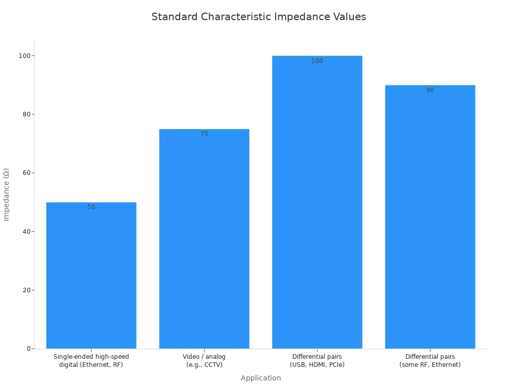
The 50Ω standard has a long history. Engineers in the 1920s and 1930s found that best power transfer happens near 30Ω. Lowest signal loss occurs near 77Ω. Highest voltage happens around 60Ω. No single value met all three goals. So 50Ω became the practical middle ground. During WWII, the Joint Army-Navy group made 50Ω the standard for compatibility. Most RF parts, amplifiers, filters, and connectors match internally to 50Ω. This makes system integration easier. On standard FR-4 boards, 50Ω traces are usually 4-10 mils wide. These widths are easy to etch reliably. Lower impedances need wide traces. Higher impedances need very thin traces that hurt manufacturing yield.
Impedance (Ω) | Signal Type / Application | Notes |
|---|---|---|
50 | Single-ended high-speed digital (Ethernet, RF) | Most common for RF and digital signals |
75 | Video / analog (e.g., CCTV) | Lower loss for long-distance analog |
100 | Differential pairs (USB, HDMI, PCIe) | Reduces EMI and improves noise immunity |
90 | Differential pairs (some RF, Ethernet) | Specific layouts require slight deviation |
Characteristic Impedance and Signal Reflections
The critical length rule tells you when you must match impedance. The critical length depends on how much you can let your target impedance differ from the actual line impedance. Larger differences allow longer critical lengths. Signal bandwidth matters. Rise time alone does not set critical length.
The critical length value depends on: 1. The difference you can allow between your target impedance and the actual line impedance. Larger differences allow longer critical lengths. 2. The signal bandwidth; any link to rise time is by chance.
For high-speed signals, you must control impedance carefully. FR-4 material creates problems here. Its dielectric constant changes with frequency. At 1 MHz, FR-4 is about 4.5. At 1 GHz, it drops to 4.0-4.2. At 10 GHz, it reaches 3.9-4.0. Polarization mechanisms cannot keep up with fast-changing electric fields. Dielectric constant limits for high-speed materials stay under 2%. For FR-4, limits can reach 10%. This change makes FR-4 bad for controlled impedance boards in high-frequency circuits.
Material | Dk at 1 MHz | Dk at 1 GHz | Dk at 10 GHz |
|---|---|---|---|
Standard FR4 | 4.2 - 4.7 | 4.2 - 4.4 | 4.0 - 4.2 |
Rogers RO4003C | Not specified | Not specified | 3.38 ± 0.05 |
Rogers RO4350B | Not specified | Not specified | 3.48 ± 0.05 |
Rogers RT/duroid 5880 | Not specified | Not specified | 2.20 ± 0.02 |
Isola Astra MT77 | Not specified | Not specified | 3.00 ± 0.05 |
Taconic TLY | Not specified | Not specified | 2.20 ± 0.02 |
Panasonic Megtron 6 | Not specified | Not specified | 3.40 ± 0.04 |
Differential Impedance and Pair Routing
Differential impedance measures the impedance between two coupled traces. High-speed routing often uses differential pairs for signals like USB, PCIe, and HDMI. These pairs carry equal but opposite signals. The receiver reads the difference between them. This method rejects common-mode noise well.
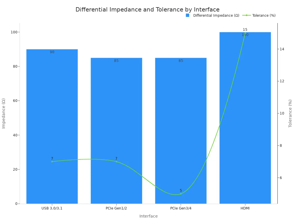
Interface | Differential Impedance Target | Tolerance |
|---|---|---|
USB 3.0/3.1 | 90Ω | ±7% |
PCIe Gen1/2 | 85Ω | ±7% |
PCIe Gen3/4 | 85Ω | ±5% |
HDMI | 100Ω | ±15% |
For USB 3.0 differential signaling, the target differential impedance is set to 90Ω. This confirms the standard requirement for this interface.
Keeping both traces the same length stops skew. Skew means one signal arrives before the other. Precise spacing between traces controls the coupling. This coupling changes the differential impedance value. You must keep both traces close together along their whole path. They should also stay the same distance from the ground plane. Any change alters the impedance. Matching impedance for differential pairs needs careful attention to shape and material properties. Signal integrity depends on this care. Your impedance control methods must account for all these factors to get reliable performance.
Design Techniques for Impedance Control
Making a PCB that works well starts with two main steps. First, you must plan the stackup with care. Then, you must follow strict routing rules. Together, these steps form the base of useful impedance control methods.
Stackup Design and Material Selection
A good stackup starts with your layer count. For many high-speed designs, a 4-layer board uses a Signal-Ground-Power-Signal setup. This setup supports 50 ohm single-ended traces and 90 to 100 ohm differential pairs. A 6-layer board puts the top and bottom layers on thin dielectrics. These outer layers carry the controlled impedance traces. Internal layers act as power and ground planes. A 10-layer board adds more signal and plane layers. The extra layers give you more space for high-speed routing and better isolation between signals.
Your material choice sets the dielectric constant, or Dk. This value, along with dielectric thickness and copper weight, sets your trace width for a target impedance. Standard FR-4 has a Dk range of 4.0 to 4.2 at 10 GHz. This wide range makes design hard for high-frequency circuits. Materials like Isola 370HR and Rogers 4350B offer much tighter Dk control. Isola FR408HR shows a Dk of 3.68 with only 0.07 change from 100 MHz to 10 GHz. This steadiness makes impedance matching easier. The loss tangent, or Df, also matters. Lower Df values mean less signal loss. FR408HR has a Df of 0.0092 at 2 GHz. This supports reliable integrity for high-speed digital links.
Copper weight directly affects your trace shape. Heavier copper requires wider traces to maintain the same impedance, and it makes etching less exact. For dense high-speed routing, you must balance trace density against signal integrity.
Glass weave style adds another factor. The glass fibers and resin have different dielectric constants, creating local Dk changes across the board. A trace over more glass moves slower; a trace over more resin moves faster. This mismatch creates skew in differential pairs. You must pick your laminate supplier with care and check process consistency.
You can use calculators for early-stage planning. The IPC-2221 based calculator gives you a starting point. But it does not capture all factors. Final trace width depends on board construction, copper distribution, and cooling conditions. For reliable results, use a field solver for final checks. These tools model the real geometry and materials well. These methods to achieve impedance matching need careful planning.
Routing Over Ground Planes and Avoiding Discontinuities
Once your stackup is set, you must route with care. Always run high-speed traces over a continuous ground reference plane. This plane gives a clear return path for the signal. It keeps a steady impedance along the whole trace. A solid reference plane is one of the best impedance control methods you can use.
Never route high-speed signals over split planes. A gap forces the return current to find a longer path. This creates an impedance break. The signal reflects at that point. Ringing and data errors follow. If you must cross a plane split, use stitching capacitors or change layers near a ground via. Avoid crossing splits whenever you can.
Trace spacing also matters for signal integrity. Adequate spacing between parallel traces reduces crosstalk. Tight spacing in HDI boards may increase crosstalk, so check your crosstalk budget with care. A gap in the reference plane makes crosstalk worse.
These methods to achieve impedance matching need discipline during layout. Plan your pcb stackup. Pick materials with tight Dk tolerances. Route over solid planes. Each step builds on the last. Skip one step, and your integrity suffers. Combine these impedance control methods with verification to get reliable results every time. Good impedance matching ensures your high-speed signals arrive cleanly at their destination.
Manufacturing and Verification for Impedance Control
Your design work does not stop when you finish the layout. The manufacturing process adds real-world changes that alter your carefully planned impedance values. Knowing these changes helps you set realistic goals and spot issues before they reach your final product.
Managing Material Tolerances and Etching Effects
Your chosen dielectric material has a tolerance on its Dk value. Standard FR-4 can change a lot, while high-speed laminates stay more stable. This change directly affects the impedance you get on the finished board. Copper weight also varies, changing trace thickness and final impedance.
The etching process removes copper to form your traces, but it does not remove material perfectly straight down. The process creates an undercut, leaving a trapezoidal shape wider at the bottom than the top. The etch factor describes this behavior. A higher etch factor means less undercut and a more rectangular trace shape.
A standard impedance tolerance works for many controlled impedance designs. Some applications need tighter limits. You should talk with your manufacturer early about tighter needs, because they affect materials, stackup, manufacturing controls, testing, cost, and lead time.
The etch factor influences the final trace width. You can work with your manufacturer to account for etch effects in your impedance calculations.
Impedance Testing and Quality Assurance
Verification starts with Time Domain Reflectometer (TDR) testing on test coupons. These coupons sit at the panel edge and show your actual trace shape. TDR testing sends a fast pulse down the trace and measures reflections. The reflections show the impedance profile along the whole length.
Panel-edge coupons give more reliable results than on-board dummy traces. On-board traces need tying reference planes together without affecting the board, use up valuable board space, and add cost if tested per board. On-board measurements can trick you because board stripline traces reach target impedances when loaded and powered, conditions that do not exist on a bare board.
Follow these best practices for good impedance testing:
Specify measurement locations, such as multiple coupons per panel, and preferred test equipment standards.
Use standard documentation to reduce confusion, including a dedicated impedance control section in the manufacturing package.
Work with the manufacturer by asking for a pre-production stackup proposal and adjusting trace widths based on TDR-verified data.
Review panel utilization, knowing that edge effects on coupons may not show inner board regions accurately, and address this early in specifications.
This verification step catches process issues early. It confirms your high-speed boards meet the impedance specifications before you start full production. Good signal integrity depends on this partnership between your design rules and your manufacturer's process controls. Your integrity goals become possible when you plan for manufacturing realities from the start.
Impedance control stands as a non-negotiable pillar of high-speed PCB design. You must master trace geometry, dielectric materials, and stackup planning. Use calculators and field solvers to verify your work before manufacturing.
Achieving consistent impedance requires partnership with your fabricator. Communicate tolerances clearly and review test coupon results together. This collaboration protects signal integrity across every board.
The industry now targets higher data rates for next-generation Ethernet and switch systems. Standards bodies like IEEE and OIF are drafting specifications for these speeds. Your impedance control techniques must evolve accordingly. Apply these principles now. Your next high-speed pcb project will demand them.
FAQ
What tolerance should I pick for my controlled impedance traces?
A standard impedance tolerance is good for most projects. Tighten it if your design needs less error. Talk to your maker early about tighter needs. They change materials, layers, testing, price, and time.
Why does my impedance change after the board is made?
The etching process does not remove copper evenly. It leaves a shape that is wider at the bottom. Your material's Dk value also differs from its data sheet. These things shift impedance from your plan. Test coupons at the panel edge with TDR testing show the real values on your finished boards.
Can I route high-speed traces over a split plane?
No. A split plane makes the return current go a longer way. This creates a break in the signal path. It causes reflections and data errors. If you must cross a split, use stitching capacitors or switch layers near a ground via.
How does glass weave style change my differential pair routing?
Glass fibers and resin have different dielectric constants. This gap creates local impedance changes across your board. One trace may sit over more glass than its partner. This causes timing skew. Different suppliers make different weave quality, so pick your source with care.
When do I need a field solver instead of a calculator?
Use calculators for early planning. They give a starting point using IPC-2221 methods. For final checks, switch to a field solver. These tools model your real shape, copper spread, and material traits with better accuracy. That matters for your high-speed pcb designs.
See Also
Enhancing Signal Integrity Through Impedance Control in PCB Fabrication
Key Process Demands for Multiple Impedance Regulation in PCB Manufacturing
Understanding High-Speed Printed Circuit Boards and Their Applications
Selecting Optimal Materials for High-Speed Circuit Board Design
