Industrial PCB Special Processing Technology
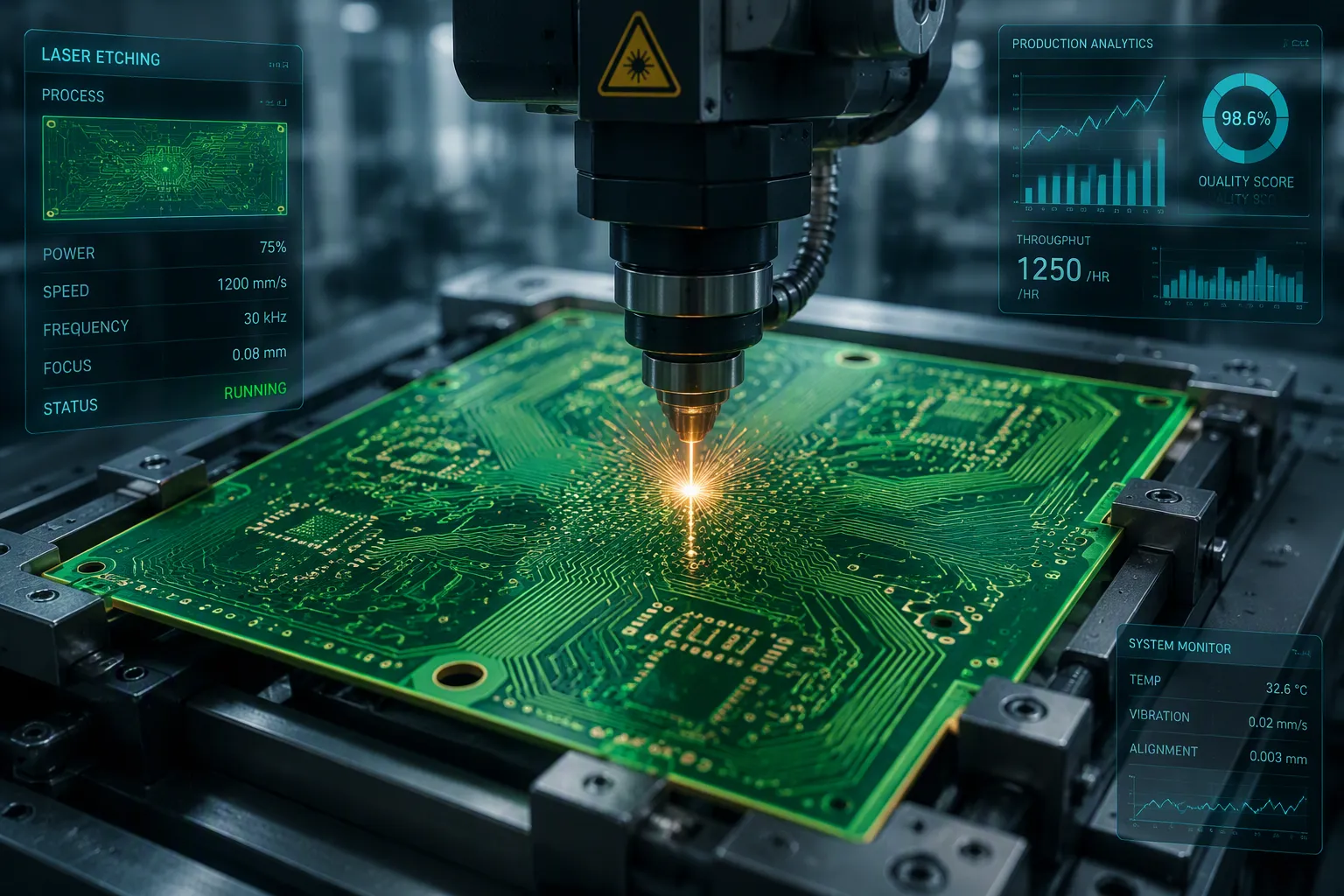
Industrial PCB special processing technology includes advanced ways to make boards that go beyond normal methods. You will see HDI, laser drilling, back drilling, impedance control, heavy copper, embedded components, ultra-thin boards, carbon oil, and flex circuits. These methods are used for special reasons.
Each method handles tough needs. You need more circuits in less space, cleaner signals, and better heat control. Hard industrial settings need more reliability. These technologies give that performance.
Your choices in processing affect everything. Design flexibility, cost, time, and quality all depend on your approach. Knowing these options helps you pick the right circuit board for your need. A good choice turns a simple board into a strong solution. Advanced PCB making opens doors that normal methods cannot.
Key Takeaways
Special techniques like HDI and laser drilling fit more circuits into tiny spaces.
Back drilling removes the extra bits in holes to keep fast signals clear.
Heavy copper boards can carry more electrical current and manage heat more effectively.
Flex circuits can bend and move many times without breaking.
Picking the right way saves money and makes it more dependable.
Special Processing Technology for Industrial PCB
HDI, Laser Drilling, and Back Drilling
High Density Interconnect (HDI) technology changes how you build a printed circuit board. You use HDI to make more connections in less space. This method uses microvia processing for tiny links between layers. Laser drilling makes these small vias possible. You can get microvia diameters as small as 0.05 mm. The usual range is 0.05 mm to 0.15 mm for dense routing. This small size lets you put connections where standard drilling cannot reach.
Aspect ratio defines the reliability of each microvia. It compares depth to diameter. For standard manufacturing, you aim for a 0.75:1 ratio. Advanced processes reach a 1:1 ratio. A 100 µm microvia should not go deeper than 100 µm. This rule ensures reliable plating and joint integrity. You must control the depth carefully during laser drilling. This high-precision step decides the final quality of your board.
Capability Level | Aspect Ratio (Depth:Diameter) |
|---|---|
Standard | 0.75:1 |
Advanced | 1:1 |
Back drilling takes out unused via stubs in high-speed circuits. These stubs cause signal reflections. You remove them with controlled-depth back drilling. The depth tolerance is ±0.002 inches. This precision matters because small changes affect the result. If you drill too shallow, you leave a longer stub. If you drill too deep, you damage functional layers. The leftover stub depth in production is 4 to 8 mils. Each 1 mil increase in stub depth adds about 0.25% loss. For a 10 Gbps design, removing a 1 mm stub reduces loss by up to 0.5 dB. You should keep the stub length below 1/10 of the operating wavelength. For 25 Gbps data in FR4, that means 2 to 3 mm maximum. This method is critical above 1 GHz. Without it, the stub acts like an antenna and distorts the signal.
Back drill depth tolerance is typically ±0.002 inches, ensuring that the stub is minimized without over-drilling into the functional layers.
These techniques together give you higher integration density and better performance for your industrial PCB designs. HDI combines with back drilling and laser drilling to create boards with unmatched routing. You choose HDI when you need small size and many connections. HDI also supports fine-pitch components. The board needs careful planning for layer stackup and via placement.
Ultra-Thin and Ultra-Thick PCBs
Board thickness extremes serve different needs. Ultra-thin PCBs work well for small devices. You find these boards in wearable industrial tools, medical devices, and miniaturized electronics. The definition of an ultra-thin printed circuit board is a thickness of 0.4 mm or less. Advanced versions can go as thin as 0.05 mm. For wearable technology, 0.2 mm is a common target thickness. These thin boards often use flexible materials like polyimide and have 1 to 2 layers. You use them in applications where space is limited. Examples include handheld sensors, smart gloves, and compact controllers.
Ultra-thick PCBs handle the opposite need. You use them in high-power industrial applications. Thick boards carry more current and dissipate heat better. They also provide mechanical strength for heavy components. Ultra-thick PCBs usually start at 2.0 mm and can go over 5.0 mm. You find them in power supplies, motor drives, and industrial converters. The extra thickness gives better heat dissipation and mechanical support for large components.
Both extremes create production challenges. For ultra-thin boards, lamination is tricky. The thin material can warp or shift during pressing. Drilling needs careful speed control to prevent tearing. Plating thin holes needs customized chemistry. For ultra-thick boards, the challenges flip. You need longer drill bits and more aggressive plating cycles. The aspect ratio of through-holes becomes hard to manage. You must adapt your advanced PCB manufacturing processes for each thickness range.
Your choice of special processing technology depends on the applications. A wearable sensor needs an ultra-thin design. A power converter needs a thick board. Both need the same attention to quality during production. The technology you pick decides the final reliability of your printed circuit board. Understanding these extremes helps you choose the right approach.
Signal Integrity, Materials, and PCB Finishes
Impedance Control and High-Frequency Materials
Impedance control keeps signals clean. You match the trace's impedance to the source and load. The goal is usually 50 ohms for single-ended lines. You change trace width and laminate thickness to reach this number. The dielectric constant (Dk) affects how fast and how far signals travel. A lower Dk of 2.2 lets signals move faster than a Dk of 4.4. The loss tangent (Df) controls how much signal is lost. A Df of 0.001 loses less than a Df of 0.02. This becomes important above 5 GHz.
Standard FR4 has a Dk around 4.3 to 4.7 and a Df around 0.02. It does not work well above 1 GHz. You need better laminates for high-frequency work. Materials like Rogers 3000/4000 series have a Dk of 2.2 to 3.5 and a Df of 0.001 to 0.003. PTFE has a Dk of about 2.1 and a Df of about 0.0003. These choices improve signal quality. You can use them with HDI technology for more routing density.
Also watch the glass weave effect on your board. The PCB uses woven glass fibers in resin. Glass has a higher Dk than resin. A trace over glass moves slower than one over resin. This causes timing differences in differential pairs. The worst case can be 4 ps per inch. Route traces at a 2.3 degree angle to reduce this. This lowers the standard deviation from about 7 ps per inch to under 1 ps per inch. Spread glass also helps by flattening fiber bundles.
A stable Dk across frequencies gives reliable impedance control. Low moisture absorption stops Dk from changing. High Tg above 170°C keeps things stable. Low CTE reduces stress on plated holes. Processing high-frequency materials the right way gives consistent results.
Surface Finishes and Carbon Oil Process
Surface finishes protect copper on your PCB. You choose the finish for your board. ENIG gives a flat surface for fine-pitch parts. It resists oxidation well. OSP provides a thin coating for lead-free soldering. Hard gold handles repeated use at connectors.
Carbon oil serves special uses. Use it for switch contacts and grounding. Screen print carbon ink onto the board. It cures into a conductive layer. You find this process in control panels and keypads. It costs less than gold plating. The board processing uses standard manufacturing steps. This technology fits many industrial uses.
Each finish fits specific needs. The choice affects cost and reliability. For high-speed designs, a flat finish matters for better signal performance.
Heavy Copper, Embedded Components, and Flex
Heavy Copper for Durable Printed Circuit Boards
Heavy copper processing solves heat and current problems in power electronics. A heavy copper printed circuit board has 3 oz or more of copper per square foot. Some makers offer up to 14 oz. For extreme needs, you can get up to 120 oz for copper planes that work as built-in heat sinks. This method fits many industrial pcb uses.
The table below shows how copper thickness changes current capacity at a steady 20°C temperature rise.
Copper Weight | Trace Width | Current Capacity | Temperature Rise |
|---|---|---|---|
1 oz | 2.5 mm | ~8 A | 20°C |
3 oz | 2.5 mm | ~18 A | 20°C |
6 oz | 2.5 mm | ~28 A | 20°C |
10 oz | 2.5 mm | ~38 A | 20°C |
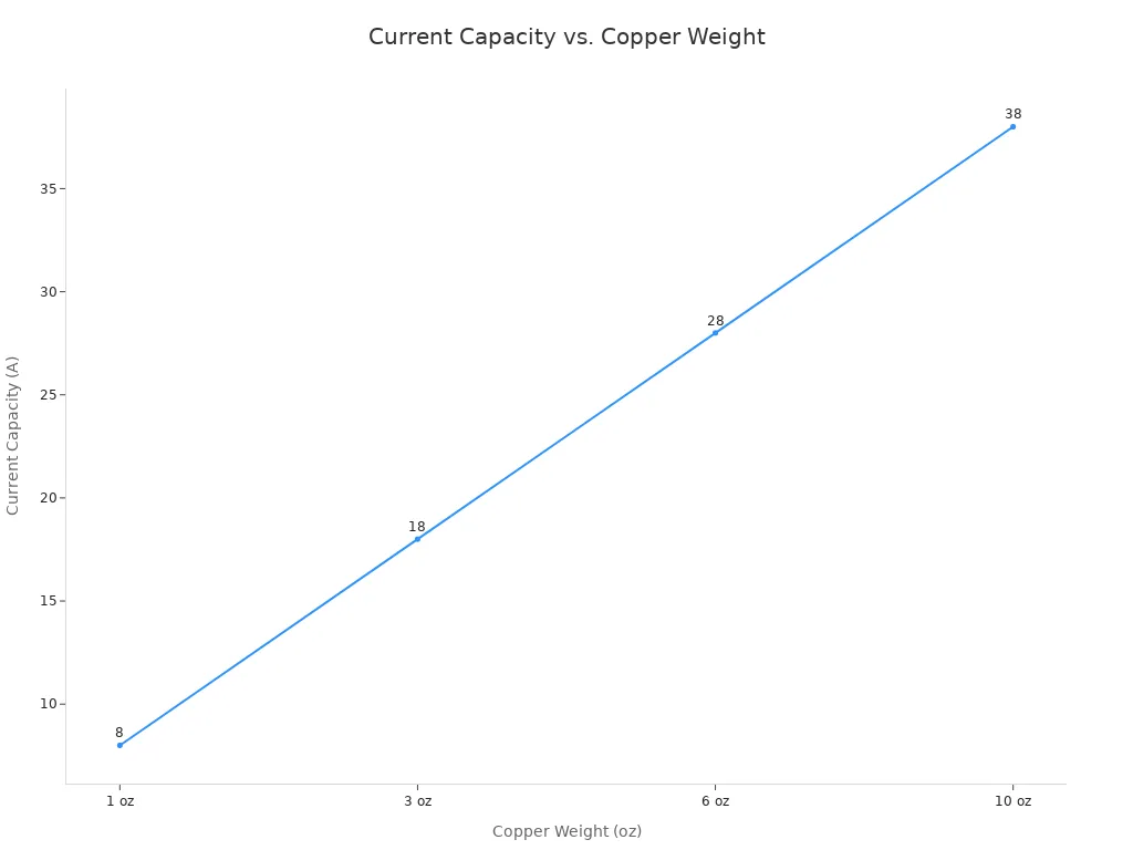
Thicker copper gives you a clear gain. A 1 oz trace carries about 8 A. A 10 oz trace carries about 38 A. So you need less board space for high-current paths. The bigger cross-section lowers resistance and heat buildup. The result is better heat control without extra cooling parts.
In real use, adding thermal vias under high-power parts on a 6 oz board can drop junction temperatures by 10-15°C. The thick copper works as a built-in heat sink. For a power supply moving 50 amps, a 6 oz board keeps temperature rises below danger points. The lower thermal resistance stops hot spots and boosts reliability.
Embedded component technology pushes this integration further on the pcb. You put parts inside the board layers instead of on top. This saves space and improves signal quality. Embedded parts pair well with heavy copper for compact power designs. Together they give you higher density and better performance. You can also use HDI methods with embedded parts for even more routing options.
Flex, Rigid-Flex, and Testing Methods
Flex circuits handle movement that rigid boards cannot. You use flex pcb technology for jobs that need bending and flexing. Polyimide-based flexible circuits offer a reliability range of 100,000 to 1,000,000+ bend cycles in dynamic applications.
A single-layer dynamic flex with the correct design can last for many millions of bend cycles, whereas the same design on a copper substrate or with a too-tight radius could fail in the thousands of cycles.
Design choices directly affect cycle life. Proper bend radius and layer count determine reliability. You must size the bend radius correctly. A too-tight radius causes early failure. A single-layer design with proper geometry can last millions of cycles. You use rigid-flex to combine flexible and rigid sections in one printed circuit board. This removes connectors and improves reliability. The final printed circuit board benefits from careful design choices.
Testing checks the quality of your flex and rigid-flex assemblies. You use several nondestructive methods to inspect solder joints.
Nondestructive Testing Method | Application to Solder Joint Inspection |
|---|---|
Visual Inspection (Manual & AOI) | Detects surface-level defects such as insufficient solder, cracks, and component misalignment. |
Automated X-ray Inspection (AXI) | Inspects concealed solder joints beneath components; reveals internal voids. |
Automatic Laser Test (ALT) | Checks solder paste volume and alignment before reflow. |
Electrical Testing (Continuity & Isolation) | Validates circuit integrity for opens and shorts without damage. |
These pcb special testing technologies ensure your board meets quality standards. X-ray inspection finds hidden defects in buried joints. Electrical testing confirms every connection works. You pick the right tests based on your needs. Proper board processing during manufacturing also affects test results.
Selecting the Right Special Processing Technology
Complexity, Cost, and Lead Time Trade-offs
Your design complexity directly shapes your budget. Simple HDI boards with lower complexity achieve initial yield rates of 95-98 percent. More advanced substrates like SLP drop to 85-90 percent. That yield gap matters because every failed board costs you money. The overhead ratio also climbs from 20-25 percent to 25-30 percent as complexity rises. You pay for that difference in every production run.
Trace width and spacing create another cost lever. Standard 6/6 mil trace and space remains the industry's cost-efficient sweet spot. Advanced designs with trace and space at or below 3/3 mil require HDI and laser direct imaging technology. That precision adds a premium to your fabrication cost. You should ask yourself whether your design truly needs that fine resolution. Many industrial pcb applications work perfectly well with standard geometries.
Laser drilling for microvias carries a significant price tag. Specialized laser drilling costs 2 to 5 times more than conventional drilling. That multiplier means a 100 to 400 percent premium over standard processes. You must weigh that expense against the density you gain. Sometimes you can avoid the premium entirely. Using blind and buried vias requires multiple lamination cycles. Avoiding them can save up to 40 percent on total fabrication costs.
Layer count drives cost per unit area more than any other factor. A typical 12-layer HDI board might need 3 to 4 separate lamination steps. Each cycle costs $50 to $100 per panel in equipment and labor. A 10-layer board designed with 2 lamination cycles instead of 3 can save approximately $30 to $50 per panel. Reducing layer counts cuts material and production costs significantly. A 4-layer HDI design can cost less than an 8-layer traditional board. That saving offsets the premium for HDI processing.
Controlled impedance routing introduces yield sensitivity. Tighter impedance targets increase cost and scrap risk. Only specify impedance tolerance as tight as required. Overly strict tolerances raise expenses without improving performance.
Early design for manufacturing review helps you align impedance goals with yield and cost. Consulting your manufacturer early balances design complexity with manufacturability. Yield is the primary driver of profit. A simpler design with higher yield often outperforms a complex one on total cost.
Material, Equipment, and Environmental Factors
Your material choices affect both performance and compliance. RoHS regulations restrict lead and other hazardous substances in electronics manufacturing. ENIG does not rely on lead in its composition. This makes it an ideal lead-free finish that aligns directly with RoHS rules. Other compliant options include immersion silver, immersion tin, OSP, soft bondable gold, and full-body gold finishes. You must verify that your chosen finish meets environmental standards for your target markets.
Equipment capability determines what processing you can attempt. CO2 lasers at 10.6 μm suit organic materials like FR-4. UV lasers at 355 nm provide finer precision for copper or mixed materials. Power output matters too. You need 10 to 20 W for thin boards and 30 W or more for thicker multilayer boards. Control software must allow adjustment of beam focus, pulse duration, and drilling depth. It must also support Gerber file compatibility. Safety features include enclosures, emergency stop buttons, and ventilation for fume handling. Entry-level systems range from $1,000 to $5,000. Industrial machines cost significantly more.
Your operating environment shapes material selection. High-temperature settings demand laminates with stable dielectric properties. Humid conditions require materials with low moisture absorption. Mechanical stress calls for flex or rigid-flex constructions. Each application brings unique demands. You match your printed circuit board technology to those conditions.
The right special processing technology balances all these factors. You evaluate density needs, signal requirements, thermal loads, and budget constraints together. A wearable sensor needs ultra-thin construction. A power converter needs heavy copper. Neither choice works for the other application. Understanding your trade-offs leads to better decisions. Your final printed circuit board performs reliably when you match processing to purpose. Quality comes from informed choices at every stage of manufacturing.
All these special processing technologies, such as HDI, laser drilling, carbon oil, and heavy copper, help you build industrial PCBs that meet tough needs in speed, reliability, and size. Each technology choice changes your design, manufacturing cost, lead time, and quality control.
Future trends point toward more miniaturization, wider use of embedded parts, and more demand for materials that handle higher frequencies and heat. You should check your own needs for density, signal speed, power, and environment against the technologies covered here. This review helps you make smart choices for your printed circuit board. The right method gives better reliability and performance for your industrial PCB uses. Your PCB works best when you match the method to the purpose.
FAQ
When should you use back drilling for your pcb?
Back drilling is needed for high-speed circuits that run above 1 GHz. It takes away unused via stubs that cause signal reflection. This method makes your board's signal work better. Keep the stub length below one-tenth of the working wavelength.
What makes HDI processing different from standard methods?
HDI uses laser drilling to make microvias as small as 0.05 mm. Standard methods rely on larger mechanical drill bits. You gain more routing density for compact designs. This method supports many pcb uses.
What challenges come with ultra-thin pcb manufacturing?
Ultra-thin boards under 0.4 mm need careful control during lamination. Thin material can bend or shift when pressed. Drilling must run at slower speeds to avoid tearing. Specialized pcb processing helps deliver reliable results.
How do ENIG and OSP surface finishes compare for your pcb?
ENIG offers a flat surface for fine-pitch parts. OSP gives a thin coating for lead-free soldering. Your printed circuit board needs should match your assembly needs and budget. This finish choice affects the total cost.
See Also
Key Factors for Producing Circuit Boards in Demanding Industrial Settings
Manufacturing Techniques for Multilayer Boards with Thick Copper Layers
Essential Materials and Quality Controls for Industrial Rigid Circuit Boards
How Multilayer Circuit Boards Are Used in Various Sectors
Utilizing Horizontal Electroless Copper Deposition in Circuit Board Fabrication
