Multi-layer PCB Lamination Design Basics

You can think of multi-layer PCB lamination as the main support for modern electronics. This process sticks copper and dielectric layers together. It makes a strong and dependable printed circuit board. You pick a multi-layer pcb when you need to put advanced technology in a small device. It helps you fit more circuits or save space in things like smartphones and laptops. Multilayer solutions also make devices work better and last longer, especially in important devices. Many people ask how the materials, structure, and steps in design and making affect how well a multilayer pcb works.
Key Takeaways
Multi-layer PCBs fit more circuits in a small space. This makes them great for devices like smartphones and laptops. They help advanced technology work better.
The layer stack-up is very important for signals and power. You must plan the order and thickness of layers with care. This helps stop problems from happening.
Use good materials for core and prepreg to make strong bonds. Good materials also help the PCB work well. Pick materials that fit your design needs.
Use DFM rules to lower mistakes and make production faster. Work with manufacturers early to help the process go smoothly.
Quality control checks, like automated optical inspection, find problems early. These checks make sure multilayer PCBs are reliable.
Multi-layer PCB Lamination Overview
What Is Multi-layer PCB
A multi-layer pcb helps you fit more circuits in a small space. This board has at least three layers of copper and insulation stacked up. Each layer does something important in your design. You can find multi-layer pcb in things like smartphones and computers. These boards help make devices smaller and stronger.
Here is a table that shows how multi-layer pcb is different from single-layer boards:
Feature | Single-Layer PCB | Multi-Layer PCB |
|---|---|---|
Structure | One copper layer on one side | Many copper layers stacked together |
Design Complexity | Simple design, easy to make | Harder design, needs careful planning |
Applications | Used in simple things like LED lights | Used in advanced things needing small size and power |
Thickness | Usually about 1.57mm, can change | Can have many layers, usually 4-12, with different thicknesses |
Vias | No vias, parts on one side | Vias connect the layers |
Material | Made from FR-4, aluminum, or CEM | Made from things like FR-4 or Rogers |
You can see that multi-layer pcb lets you add more features and make things work better without making the board bigger.
Laminate Structure and Function
When making a multi-layer pcb, you stack copper and dielectric layers. The laminate keeps these layers together. Each layer has its own job. The power plane gives voltage to parts. The ground plane helps stop electromagnetic interference and keeps signals clear. Inner signal layers connect different parts of the circuit.
Here is a table that shows what each layer does in a normal pcb stackup:
Layer Type | Function |
|---|---|
Ground Plane | Helps stop electromagnetic interference |
Power Plane | Gives voltage to parts |
Inner Signal Layer | Connects different parts of the circuit |
The laminate makes sure all the layers stay stuck together. This strong hold gives good electrical connections and helps the product work well. When you use multi-layer pcb, you get better signals, less interference, and more connections in a small space. These things help you build better technology that works well.
PCB Lamination Process
When you make a multi-layer pcb, you must be careful. Each layer needs to line up and stick together well. This process helps you build circuit boards that are strong and reliable. These boards work well in fast designs and advanced technology.
Layer Stack-up Steps
You begin with the pcb layer stackup. This means you plan where each layer goes in the board. You pick the order for copper, prepreg, and core materials. Every layer has its own job. Some layers carry power. Some layers carry signals. Others act as ground. Good stackup planning helps you control how signals move and how power flows. It also keeps your multilayer pcb stable and cuts down on noise.
Here is a table showing the main steps in making a multilayer pcb and what equipment you need:
Step Number | Step Description | Equipment Required |
|---|---|---|
1 | Design and Engineering | Design software, tooling films |
2 | Material Selection and Preparation | Copper-clad laminates, prepreg |
3 | Inner Layer Imaging | Photosensitive dry film, UV light |
4 | Etching | Chemical etching solution |
5 | AOI for Inner Layers | AOI testing equipment |
6 | Lamination | |
7 | Drilling | CNC drilling machine |
8 | Plating | Plating solution, electric current |
9 | Outer Layer Processing | Etching and imaging equipment |
10 | Solder Mask Application | Liquid photoimageable solder mask |
11 | Silkscreen Printing | Silkscreen or inkjet printer |
12 | Surface Finish | Surface finish materials |
13 | Electrical Testing and Profiling | Electrical testing equipment |
14 | Final Quality Inspection and Packaging | Inspection tools, packaging materials |
Stackup and layer arrangement happen early in the process. If you plan the stackup well, your multilayer pcb works better and lasts longer. The laminate bonds each layer tightly. This is important for fast designs.
Tip: Always check your pcb layer stackup before pressing. If you make a mistake, you can have problems with signal, power, or the whole board.
Pressing and Bonding
After stacking the layers, you press and bond them. This step uses heat and pressure to join all layers into one board. You put the stackup in a lamination press. The press heats the board to a high temperature and pushes hard. For FR-4 materials, you need a peak temperature between 180°C and 190°C. For high-Tg materials, you may need up to 200°C.
The press uses a lot of force. Most multilayer pcb manufacturing uses about 300 psi of pressure. Some presses use 200 to 500 psi, depending on the laminate thickness and type. The pressing cycle lasts about 90 minutes. This lets the prepreg melt and flow. It fills gaps and bonds each layer together.
You must control temperature and pressure carefully. If you use too much or too little, you can get problems like delamination or warping. Good compression keeps layers flat and connections strong. This step is very important for multilayer pcb design. It helps you get top performance in advanced technology.
Note: If you want your multilayer pcb to work well in fast designs, you must do pressing and bonding right. This helps your circuit boards handle fast signals and power without trouble.
When you follow these steps, you get a strong, reliable multi-layer pcb. Each layer stays in place. The whole board works as one. This process helps you build products that last longer and perform well.
Multilayer PCB Materials
Core and Prepreg
To make a multilayer pcb, you stack core and prepreg materials. The core is a strong base with copper on both sides. Prepreg is fiberglass soaked in resin. When you heat and press the stack, prepreg melts and sticks layers together. This makes a tough printed circuit board for complex designs.
Here is a table showing common core and prepreg materials and their properties:
Material Type | Typical Properties |
|---|---|
Standard FR4 Core | Low cost, good mechanical strength, stable processing, wide availability |
High TG Core Materials | Improved thermal stability, reduced Z-axis expansion, better reliability |
High-Speed Core Materials | Specialized low-loss cores for high data rates |
Low Resin Prepreg | Improved thickness control, reduced resin flow, better dimensional stability |
High Resin Prepreg | Better filling capability, improved bonding, enhanced dielectric spacing |
You pick core and prepreg based on your multilayer pcb needs. For fast designs, use high-speed core materials for good signal quality. If you need heat resistance, high TG cores are best. Prepreg type affects how well layers stick and how flat the board stays.
Tip: Always match core and prepreg to your pcb layer stackup. This helps you avoid warping and keeps your multilayer pcb process smooth.
Copper and Dielectric
Copper and dielectric materials are important for multilayer pcb performance. Copper makes the traces and planes that carry power and signals. Dielectric materials separate copper layers and control how signals move.
Pick copper thickness for each layer’s job. For signal layers, use 0.5 or 1 ounce copper. This helps with fine lines and impedance control. For power and ground layers, use 1 or 2 ounce copper to lower voltage drop. Always check how much current each layer can handle. Run thermal tests to keep your board cool.
Dielectric materials include FR4, polyimide, PTFE, and more. Each type has its own properties:
Material Type | Properties | Applications |
|---|---|---|
FR4 | Mechanical strength, electrical insulation | General use |
Polyimide | High-temperature resistance, flexibility | Flexible PCBs |
PTFE | Low dielectric constant, minimal signal loss | High-frequency circuits |
Rogers laminates | High-frequency performance, thermal stability | Advanced applications |
Metal core PCBs | Excellent heat dissipation | Power electronics, LED lighting |
Higher dielectric constants slow signals and cause timing skew.
Low-loss materials like PTFE keep signals strong over long distances.
Stable dielectric constants help reduce impedance changes and crosstalk.
When picking materials, follow environmental rules. Many laws limit dangerous substances and require eco-friendly laminates. Look for halogen-free or recyclable materials to meet these standards.
Note: New technology brings low-temperature laminating materials and ultra-low loss laminates. These help you build multilayer pcb for advanced uses and support quality control.
Multilayer PCB Design Considerations
Layer Count and Arrangement
When you design a multilayer pcb, you first pick the number of layers. The layer count changes how your board handles signals and power. It also affects how well your board works. In fast designs, small changes in layer thickness can slow signals or make them unclear. You want a stackup with even thickness to keep signal loss low and control impedance. How you arrange copper and dielectric layers decides how signals move, how power spreads, and how well your board blocks interference.
Here are some key things to remember:
Layer thickness matters for good electrical performance.
Balanced stackup helps your board stay strong and reliable.
Layer arrangement changes how signals travel and stops interference.
Fast designs need exact layer thickness to avoid noise and timing problems.
You should use best practices for stackup and layer arrangement. The table below gives a checklist for making a good multilayer pcb:
Checklist Item | Requirement / Target |
|---|---|
Copper weights should match on both sides of the core | |
Reference Continuity | High-speed signals must not cross ground plane splits |
Return Vias | Stitching vias should be at every layer change |
3W Spacing | Use for all clocks and data strobes |
Annular Ring | At least 0.15 mm wide |
Fiducials | Three global fiducials on each surface |
Always keep stackup symmetry. Even material from the center out stops the board from bending or twisting during lamination.
Signal and Thermal Management
You must manage signals and heat in every multilayer pcb. Good signal management keeps your devices fast and steady. Use ground planes for shielding, keep enough space between traces, and control impedance. Differential pair routing helps block noise in fast designs.
Technique | Description |
|---|---|
Use Ground Planes for Shielding | Put a ground plane close to signal layers to shield and cut interference. |
Maintain Proper Trace Spacing | Keep enough space between traces to lower crosstalk. |
Controlled Impedance | Make traces with steady impedance to stop signal loss and reflection. |
Use Differential Pair Routing | For fast signals, use differential pair routing to block noise. |
Managing heat is just as important. You can spread heat by using more copper and adding thermal vias. Inner layers can help move heat away from hot spots. Pick materials that carry heat well and put thermal vias near important parts. This keeps your multilayer pcb cool and strong.
Use more copper to spread heat better.
Add thermal vias to connect hot spots to inner layers.
Choose materials that move heat away from sensitive parts.
Good signal and heat management in your multilayer pcb makes your board work well and last longer.
Lamination Best Practices
Manufacturability
You can make multilayer boards easier to build by using smart design steps. Share your design files with your manufacturing partner early. Ask them for advice to find problems before making the boards. Many manufacturers give free DFM checks. These tools help you catch mistakes before they cost a lot of money.
Here are some important things to do for good multilayer boards:
Use DFM rules to stop errors and get more good boards.
Place parts in smart spots to save space and lower defects.
Route traces the right way to stop shorts and open circuits.
Pick materials that work well and do not cost too much.
Talk often with your manufacturing partner to find problems early.
Practice | Benefit |
|---|---|
Implementing DFM principles | Cuts down on errors and soldering problems. You get more good boards. |
Optimizing component placement | Saves space and lowers the chance of mistakes when putting parts on. |
Proper trace routing | Stops shorts and open circuits. This makes the board work better. |
Selecting appropriate materials | Balances how well the board works and how easy it is to make. |
Collaborating with manufacturing partners | Finds problems early so you do not waste money. |
Tip: Always follow your manufacturer's design rules. If traces are too close, you can get shorts. If pads are the wrong size, soldering may not work. Vias in bad spots can make open circuits. Check high-current paths and use DFM tools for best results.
Picking the right materials and layer setup is important. For most low- to mid-frequency multilayer boards, FR4 is a good choice. For high-frequency or special tech, you may need other materials to keep signals clear.
Quality Control
Quality control makes sure your multilayer boards are strong and last long. You need to check every layer for problems after lamination. Use special inspection tools to find issues early.
Inspection Technique | Description |
|---|---|
Automated Optical Inspection (AOI) | Finds surface problems and checks if layers line up. |
Impedance Testing | Checks electrical parts to find lamination problems. |
Microsection Analysis | Looks closely at how well layers stick and the material quality. |
AOI helps you find surface problems and layers that do not line up.
Impedance testing checks if the board’s electrical parts are right.
Microsection analysis shows how well the layers are stuck together.
For multilayer pcb making, you must keep tight rules, especially for HDI designs. Good quality control stops delamination, warping, and signal loss. This makes sure your multilayer pcb works well for new technology.
Lamination Methods Comparison
When you make multilayer boards, you must pick the right lamination method. How you join layers changes how strong, expensive, and good the board is. There are two main ways: sequential lamination and simultaneous lamination. Each way has its own steps and best uses.
Sequential Lamination
Sequential lamination is used for boards with many layers or special features. You build the board in parts. First, you press a few layers together. Then you add more layers and press again. You keep repeating this until all layers are done. This helps you make boards with lots of connections for signal and power.
Here is a table that shows how sequential lamination is different from conventional lamination:
Method | Process Complexity | Yield Rates |
|---|---|---|
Sequential Lamination | Harder, needs skilled work and many steps | More defects (3-7%) because layers must line up |
Conventional Lamination | Easier, costs less, for simple boards | Fewer defects (2-5%) for basic designs |
Sequential lamination gives you some good things. You can use shorter via stubs and smaller via holes. This keeps your design small and keeps trace width low. But it costs more and you can only add a few layers at a time.
Advantages | Disadvantages |
|---|---|
Shorter via stubs, easier via models | Costs more than standard lamination |
Smaller via holes | Only two or three layers per cycle |
Keeps minimum trace widths | Limits on reliability |
Tip: Use sequential lamination for boards with lots of layers or when you need special via shapes.
Simultaneous Lamination
Simultaneous lamination, also called conventional lamination, presses all layers at once. You stack the core, prepreg, and copper layers, then press them in one step. This works best for boards with fewer layers or simple designs. It costs less and is faster because you only press once.
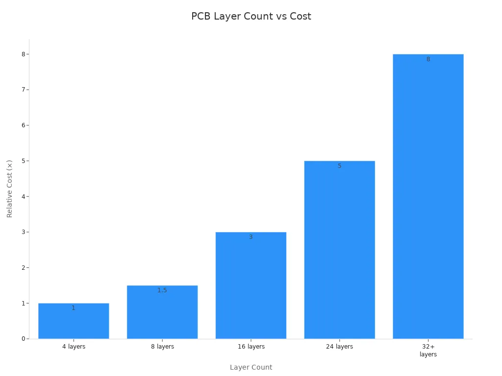
If you add more layers, cost and time go up. A 4-layer board costs the least and takes about a week. A 32-layer board can cost much more and take up to a month. Skip vias save money because they need fewer pressing steps. Stacked blind vias cost more since they need more steps and materials.
You should pick the lamination method that fits your board’s technology, layer count, and performance needs. The right choice helps you save money, get more good boards, and make your design work best.
Multilayer PCB Challenges
Delamination Issues
Delamination can happen when making multilayer boards. This means the layers do not stay stuck together. If this happens, your project may slow down. The board might not work as well. Delamination often happens if you use the wrong heat or pressure. It can also happen if there is too much water, bad materials, or rough handling.
Here are the main reasons for delamination in multilayer boards:
High heat or quick temperature changes can stress the board.
Water or wet air can get inside and cause problems.
Using bad or cheap materials makes layers weak.
Mistakes during lamination can cause layers to come apart.
Dirt or harsh places can hurt the board.
Bending or dropping the board can break the layers.
Old materials may not stick well anymore.
You can stop delamination by doing these things:
Plan your design to handle heat and space.
Pick good materials for every layer.
Watch the lamination process and clean surfaces well.
Check your boards and test them for problems.
If something fails, find out why and fix it.
The table below shows how delamination is different from other problems in multilayer PCB making:
Challenge | Description | Impact on Time |
|---|---|---|
Delamination | Layers do not stick because of wrong heat or pressure. | Adds 1-3 days to timeline |
Resin Flow Issues | Too much or too little resin makes holes or thick spots. | Delays production by 24-48 hours |
Warping | Uneven cooling or wrong materials bend the board. | Must remake, costing more time and work |
Tip: Keep your multilayer boards dry and handle them gently to stop delamination.
Warping and Misalignment
Warping and misalignment can cause big trouble in multilayer boards. Warping means the board bends or twists. This can happen if the board cools unevenly or uses the wrong materials. If your board warps, parts may not fit right. Soldering can go wrong. Warping can cause up to 25% of failures in packed boards.
Misalignment means the layers do not match up. If the board gets thicker by more than 0.2 mm, layers may not stick well. This can make empty spaces and break signal or power paths.
Rules like IPC-6012 say boards should not bend or bow more than 0.75%. This helps keep boards strong and ready for new designs.
Note: You can stop warping and misalignment by using even layer thickness, picking good materials, and watching the lamination process.
If you look out for these problems and use good steps, your multilayer boards will last longer and work better.
You can make strong multilayer boards by using smart steps. Be careful with materials. Set the press to the right settings. Check each layer to see if it sticks well. These multilayer pcb design tips help stop signal loss. They also keep power steady. New technology, like thinner dielectrics, makes boards work better. Better drilling also helps performance. If you want to learn more, look at these resources:
Resource Title | Key Focus Areas |
|---|---|
PCB Lamination Technology: A Comprehensive Guide to Multilayer Board Manufacturing | Advanced lamination challenges and specialized applications |
Planning a Multilayer PCB Stackup | Material data for stackup planning and thermal management |
FAQ
What is multilayer pcb laminate technology?
Multilayer pcb laminate technology joins copper and dielectric layers together. This makes one strong board. It helps you build advanced electronics. These boards need to work well and last a long time.
How does stack-up design affect board performance?
Stack-up design controls how signals move in your board. You can plan the order and thickness of each layer. This lowers noise and makes signals clearer. Good stack-up design helps circuits work better.
Why should you follow pcb design guidelines?
You should follow pcb design guidelines to stop mistakes. These rules help you place parts and route traces. They also help you pick the right materials. Following guidelines saves time and money.
What is a high-density interconnect?
A high-density interconnect uses tiny traces and vias. This lets you fit more connections on your multilayer board. You can make smaller and faster devices with more features.
How do you choose a layer stackup strategy?
You pick a layer stackup strategy based on your circuit needs. Think about signal speed, power delivery, and heat management. A good strategy stops problems and helps your board last longer.
See Also
An In-Depth Look At The Creation Of Multilayer PCBs
Essential Skills For Designing Multilayer PCB Circuit Layouts
Diverse Uses Of Multilayer PCBs In Various Industries
Understanding The Production Of Rigid-Flex Multilayer Circuit Boards
Challenges In Manufacturing And Prototyping Multilayer Circuit Boards
