PCB Impedance Control Explained for Beginners
PCB impedance control is about managing how signals travel in your pcb design. You must keep impedance steady so signals do not bounce back. This helps your circuits work well. Imagine water moving in pipes. If pipes change size, water splashes and slows down. In PCB circuits, sudden changes make signals bounce and lose power. Studies show keeping impedance the same everywhere helps signals stay strong. Controlling dielectric thickness also keeps signals clear in fast designs.
Evidence Description | Key Points |
|---|---|
Consistent Impedance is Critical Across Rigid and Flex Zones | Keeping impedance the same stops signals from bouncing and losing power in fast circuits. |
Controlled Dielectric Thickness Matters More Than You Think | Exact impedance is important for fast protocols. It depends on careful control of dielectric thickness. |
Key Takeaways
Keep impedance steady so signals do not get weak and circuits work right.
Control dielectric thickness to keep signals clear in fast designs.
Use certain impedance values like 50Ω for single-ended signals and 100Ω for differential pairs.
Watch trace width, dielectric material, and copper thickness to keep impedance the same.
Use tools and calculators to design PCBs with the right impedance for strong signals.
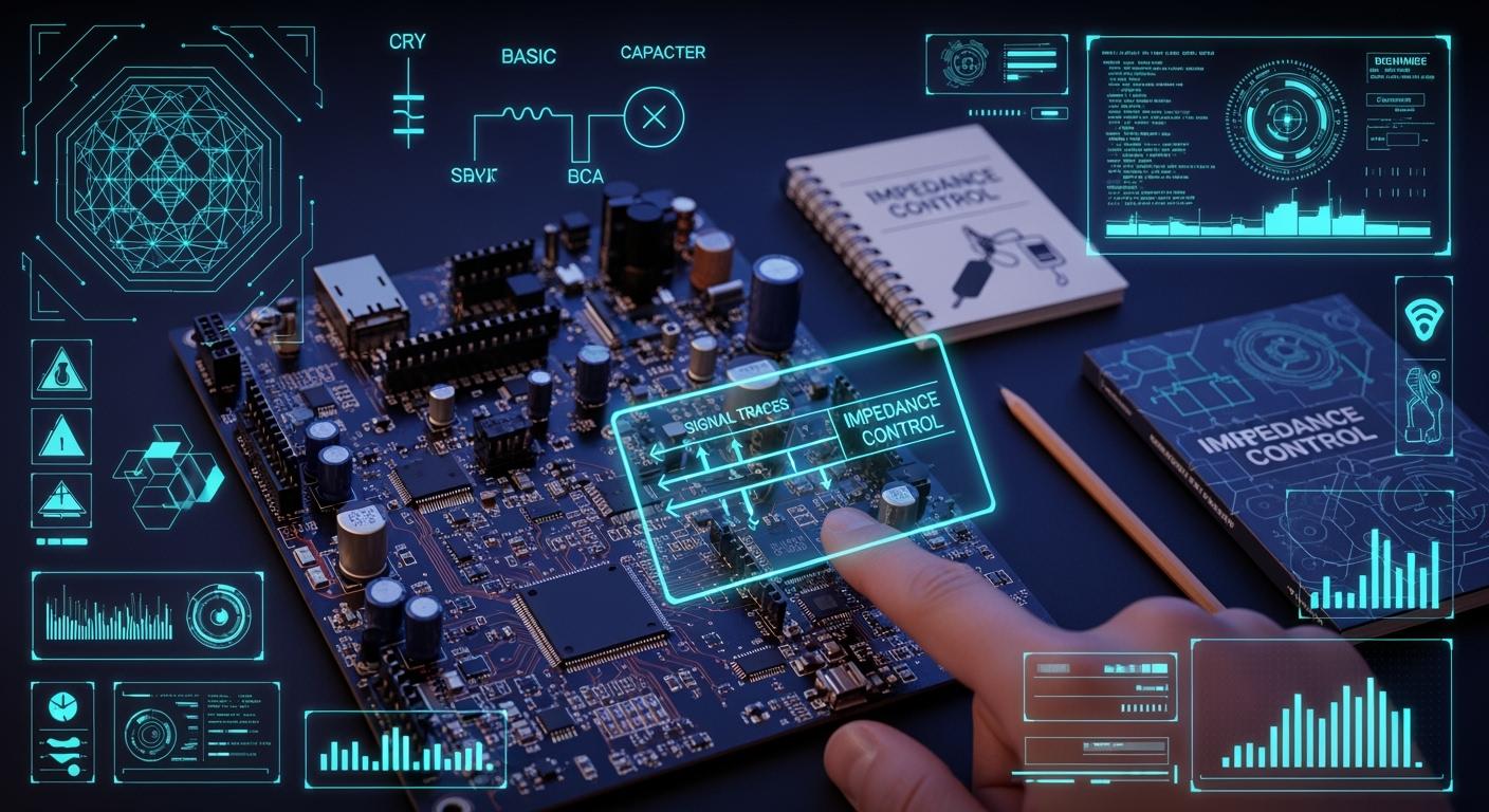
What Is PCB Impedance Control?
Impedance Basics in PCBs
Impedance is like a barrier for signals moving in a pcb trace. It is not just resistance. It also includes capacitance and inductance. These three things together affect how signals travel. When you make a pcb, you want the impedance of each trace to stay the same all the way. This keeps your signals strong and clear.
If you change the trace width or the material below it, impedance changes. This can cause problems for your signals. Books about electrical engineering say you must keep impedance steady in fast pcb designs. Having the same impedance from start to end is very important. Sudden changes, like from component pads, can hurt your signals. You can use special tricks, like reference plane cut-out, to fix these problems.
Think of impedance as a road for cars. If the road gets wider or smaller, cars might slow down or crash. In a pcb, signals are like cars. They need a smooth road with the same impedance to move safely.
Why Controlled Impedance Matters
You need pcb impedance control to keep signals safe. Fast signals can have trouble if impedance changes even a little. If you do not control impedance, signals can bounce back or get messed up. This can cause data mistakes or even make things stop working.
Common values are 50 ohms for single-ended RF and high-speed digital lines, 90 or 100 ohms for differential pairs, and other values based on protocol rules.
Most fast digital pcb traces use 50 ohms for single-ended signals. Differential pairs, like USB or Ethernet, often use 100 ohms. These numbers help keep signals strong and lower the chance of mistakes.
50Ω for single-ended signals, used in RF and fast digital lines.
100Ω for differential pairs, used in USB, Ethernet, and PCI Express.
You must use these values so your pcb works with new devices. If you do not, you might lose signal strength and have design problems.
Signal Integrity and Reflections
Signal integrity means your signals reach the end without losing shape or power. If impedance does not match, signal integrity can be lost. When a signal hits a change in impedance, some of it bounces back. This is like yelling in a canyon and hearing an echo. In a pcb, these echoes can mix with new signals and cause problems.
Here are some common problems from impedance mismatch:
Signal reflection can cause data mistakes or stop communication.
Timing problems happen when signals arrive at different times, which is bad for fast systems.
Data can get messed up, leading to errors when sending information.
Impedance mismatch causes reflections, which can mess up signals and cause data errors. Reflections happen when a signal finds a change in impedance, making voltage go too high or too low. The reflection coefficient shows how bad the mismatch is. Bigger mismatches make bigger reflections.
Cause of Reflection | Description |
|---|---|
Impedance Mismatch | Happens when a signal finds a sudden change in impedance, causing reflections. |
Changes in Trace Width | Quick changes in trace width can make impedance mismatches. |
Presence of Vias | Vias can make sudden changes that cause signal reflections. |
Connectors | Connectors can also make impedance mismatches, causing reflections. |
Unterminated Lines | Lines that are not ended right can send signals back to the start. |
You must watch pcb impedance control to keep signals strong. This helps your circuits work faster and better. When you design with controlled impedance, you make sure your signals stay clear from start to finish.
Factors Affecting Controlled Impedance
When you design a pcb, you need to control some things. These things help keep impedance the same. They change how signals move in each trace. If you do not watch them, your pcb might not work right.
Trace Width and Thickness
Trace width and thickness change impedance a lot. If you make a trace wider, impedance gets lower. If you make it thinner, impedance gets higher. Even a small change in width can change impedance a lot. Microstrip traces are on the outside of a pcb. They are very sensitive to width changes. Stripline traces are between layers. They also change impedance when you change width. But they must be thinner for the same impedance.
Wider trace means lower impedance
Narrower trace means higher impedance
Small width changes can make big impedance changes
You should check trace width and thickness to keep your pcb working well.
Dielectric Material and Layer Stackup
The stuff between pcb layers is called dielectric. The dielectric constant, or Er, shows how well it stores energy. Different materials have different dielectric constants. FR4 and PTFE are two examples. Small changes in Er can change impedance a lot. How you stack the layers, called stackup, also changes impedance.
Material | Dielectric Constant (Er) | Effect on Impedance |
|---|---|---|
FR4 | 4.4 | Standard, common in pcbs |
PTFE | 2.1 | Lower Er, higher impedance |
If you use a material with a higher Er, impedance goes down. If you use a lower Er, impedance goes up. You need to pick the right material and stackup for your target impedance.
Spacing and Copper Thickness
The space between a trace and the reference plane changes impedance too. If you make the space bigger, impedance goes up. If you make the space smaller, impedance goes down. Copper thickness matters as well. Thicker copper lowers impedance a little. For example, if you make copper 10% thicker, single-ended impedance drops by about 1–2% in multilayer pcbs. This is less than the effect from width or dielectric changes. But you still need to check it.
Tip: Always look at your pcb manufacturer’s rules for trace width, spacing, and copper thickness. This helps you keep impedance steady.
If you know about these things, you can design pcbs with the right impedance. This keeps your circuits fast and strong.
PCB Impedance Control Process
When Is Impedance Control Needed?
You need pcb impedance control for fast or sensitive signals. Many new devices use high-speed digital or radio signals. These signals need steady impedance to work right. You should use impedance control for:
High-speed digital signals like USB, HDMI, PCIe, Ethernet, SATA, and DDR memory
RF signals in wireless devices
Precision analog signals in measurement equipment
If your pcb has these signals, you must control impedance. This helps stop signal loss or errors.
How to Achieve Controlled Impedance
You can get controlled impedance by planning your pcb stackup and trace shape. First, pick the right materials and layer order. Use a controlled stackup to keep dielectric and copper thickness steady. Then, set trace width and spacing to match your target impedance. Use calculators to check your trace design. During making, manufacturers use Time Domain Reflectometry and network analyzers to test impedance and find problems.
Controlled stackup: Set layer order, dielectric thickness, and copper thickness
Controlled impedance: Change trace width and spacing to match your target impedance
Testing: Use TDR and network analyzers to check impedance
Specifying Requirements for Manufacturing
You must give your pcb maker clear details for impedance control. This helps them build your board the way you want. Makers need info about your stackup, materials, and testing. Here is what you should give:
Requirement Type | Description |
|---|---|
Stack-Up Specifications | Detailed layer setup, including signal and plane layers, board thickness, and mask layers. |
Material Properties | Things like dielectric constant, glass transition temperature (Tg), and loss tangent. |
Testing Methods | Use of test coupons and TDR checks to verify transmission line impedance. |
Tools and Calculators for Designers
You can use online tools to help with pcb impedance control. Sierra Circuits’ Impedance Calculator gives good results for trace design. Altium’s calculators use trusted formulas for microstrip and stripline traces. These tools help you set the right trace width, spacing, and stackup for your pcb. Altium’s calculators use equations that work well for low GHz signals and help you reach your target impedance.
Tip: Always use a calculator before you finish your pcb layout. This step helps you avoid mistakes and keeps your signals strong.
Applications and Risks of Ignoring Impedance
High-Speed and High-Frequency Uses
Controlled impedance is needed in many fast pcb designs. Fast signals can have big problems if impedance changes. Here are some places where you must control impedance:
High-speed digital applications
RF communication circuits, like mobile phones, Wi-Fi, and Bluetooth
High-quality analog video systems
USB connections, especially USB 3.0 and newer
HDMI for high-definition video and audio
Ethernet for network devices and cables
PCIe and DDR memory in computers
These pcb uses move data very quickly. If you do not control impedance, signals can bounce or get weak. This can make your device slow down or stop working.
Industries That Need Controlled Impedance
Many industries need pcb designs with controlled impedance. These rules are important where speed and quality matter a lot. Some main industries are:
Telecommunications, where data travels far
Computing, when signal frequencies go above 100MHz
High-speed digital and RF communication systems
High-quality video standards, like HDMI and Gigabit Ethernet
High-performance pcb manufacturing for energy-saving devices
You must follow strict rules in these fields. Controlled impedance keeps signals clear and strong in every pcb you make.
Problems from Poor Impedance Control
If you do not control impedance in your pcb, you can have many problems. Bad impedance control can cause signal reflections and crosstalk. These problems often come from changes in trace width, material issues, or copper roughness inside the pcb. When impedance changes, signals lose shape and power. This can cause data errors, slow speeds, or even system failure.
Note: You can stop most of these problems by checking your pcb design and working with your manufacturer. Always test for impedance before you finish your pcb.
When you control impedance, you protect your pcb from common problems. You help your devices work fast and stay reliable.
You can make your PCB designs better by watching impedance control. Always tell your manufacturer what impedance you need. Give them clear stackup diagrams. This helps stop mistakes and keeps signals strong. Use calculators and simulation tools to check your design. Follow trusted guides like IPC-2221. Ask for help if you are not sure.
Tell your manufacturer your target impedance and how to test it.
Use good design guides and keep learning new tools.
If you do these things, your boards will last longer and work well.
FAQ
What does "controlled impedance" mean in PCB design?
Controlled impedance means you pick a certain impedance for some traces. You keep this value the same along the whole trace. This helps signals move smoothly and not lose power. It is important for fast or sensitive signals.
How do you know if your PCB needs controlled impedance?
You need controlled impedance if your board uses fast signals. Examples are USB, HDMI, or Ethernet. If signal speed is more than 100 MHz, you should check impedance.
Can you measure impedance on a finished PCB?
Yes, you can measure impedance with a tool called a Time Domain Reflectometer (TDR). Your manufacturer can use this tool to test your board. They can show you the results.
What happens if you ignore impedance control?
If you do not control impedance, signals can bounce or get weak. This can cause mistakes in data, slow down your device, or even make it stop working.
See Also
Enhancing Signal Integrity Through Impedance Control Techniques
Essential Requirements for Multi-Impedance Control in PCB Fabrication
Exploring Rogers R4350B, R4003, and R5880 for RFPCB Applications