How to Avoid Common Silkscreen Mistakes in PCB Design

You can make silkscreen mistakes when you design pcb layouts. Some common problems are missing details, silkscreen covering pads, and hard-to-read letters. These problems make circuit boards tough to put together and can cause errors. If you follow Silkscreen Design Rules for the silkscreen layer, you help make clear pcb silkscreen markings. This stops confusion. Clear silkscreen helps with assembly and lowers expensive mistakes.
Mistake Type | Description |
|---|---|
Missing or unclear information | Important details like which way parts go and polarity marks can be missing. This can cause errors. |
Overlapping silkscreen on pads | Silkscreen on pads can melt into solder joints and cause trouble. |
Illegible character sizes | Letters must be big enough to read. If not, they can cause problems. |
Key Takeaways
Always follow silkscreen design rules. This helps you avoid mistakes. Clear markings make things easier to read. It also lowers the chance of errors during assembly.
Pick the right font size and line width. Make sure the height is at least 1.0 mm. The width should be at least 0.15 mm. This makes the text easy to see.
Keep silkscreen away from pads and vias. This stops problems when soldering. It also keeps connections strong.
Use colors that stand out for silkscreen. Put white on dark backgrounds. Put black on light backgrounds. This makes everything easier to see.
Check your design with a checklist before making it. This helps you find mistakes early. It also makes your PCB more reliable.
Silkscreen Design Rules
You need to follow silkscreen design rules to make sure your pcb is easy to read and build. These rules help you avoid mistakes that can slow down manufacturing or cause errors during assembly. Good pcb silkscreen design makes your board look professional and helps workers place parts in the right spots.
Font Size and Line Width
You should always use the right font size and line width for your silkscreen. If you make the lines too thin or the letters too small, the text can disappear during printing. This makes it hard for anyone to read the markings on your pcb. Most pcb manufacturers follow industry guidelines for silkscreen design rules. You can see the most common values in the table below:
Parameter | Minimum Value | Recommended Value |
|---|---|---|
Font Size | 1.0–1.5 mm (40–60 mil) | — |
Line Width | 0.15–0.20 mm (6–8 mil) | — |
Silkscreen Clearance | 0.1–0.15 mm (4–6 mil) | — |
You should never use a line width less than 0.15 mm (6 mils). Features thinner than this can break or fade during the silkscreen process. For high-density pcb layouts, you can use a reference designator like "C12" at 0.050 inches with a 0.006-inch line width. This keeps the text clear for assembly workers.
Tip: Always check with your pcb manufacturer for their exact silkscreen design rules. Some factories may have special requirements.
Text Height and Spacing
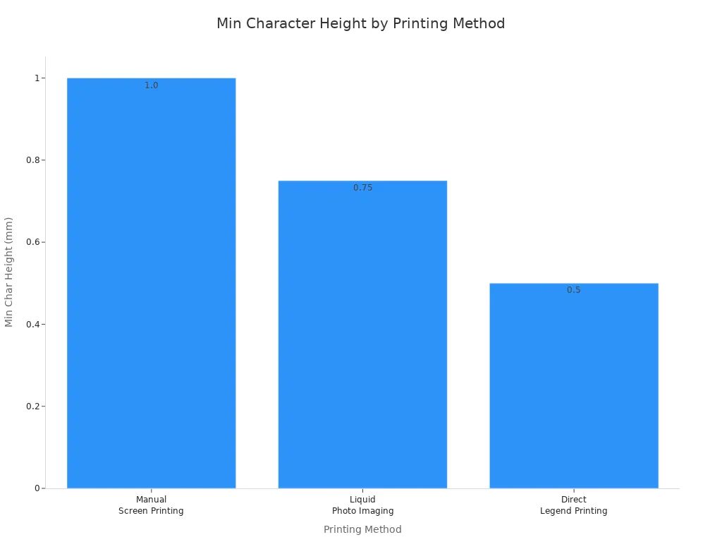
You must use adequate text size and spacing to keep your silkscreen readable. If you crowd letters together or make them too small, you risk confusion during assembly. The table below shows the best guidelines for text height and spacing based on different printing methods:
Printing Method | Minimum Character Height | Minimum Line Width | Notes |
|---|---|---|---|
Manual Screen Printing | 0.040" (1.0mm) | 7 mil | Use as large font size and line width as possible without going smaller than 50 mil font size and 7 mil line width. |
Liquid Photo Imaging (LPI) | 0.030" (0.75mm) | 4 mil | Suitable for finer resolution. |
Direct Legend Printing | 0.020" (0.5mm) | Finest resolution | Best for high precision applications. |
Standard Silkscreen Printing | N/A | N/A | Maintain minimum 0.15mm spacing between text and component bodies. |
You can see from the chart below that different printing methods allow for different minimum character heights:
You should always keep at least 0.15 mm between silkscreen text and any pads, holes, or traces. This helps prevent ink from bleeding into important areas. If you follow these silkscreen design rules, you will avoid many common problems.
Use a minimum line width of 4 mils for reliable printing.
Never use features narrower than 4 mils.
Keep at least 6 mils of space between silkscreen and any exposed metal.
Color and Font Type
You need to choose the right pcb silkscreen colors and font types for your design. The color of your silkscreen should stand out against the solder mask. This makes the text easy to read. Most pcb manufacturers use white silkscreen on green, blue, or black solder masks. If your board uses a light solder mask, you should use black silkscreen. Some colors, like pink, are hard to read and can cause problems during manufacturing.
Color | Application/Notes |
|---|---|
White | Best contrast on dark solder masks (green, blue, black) and widely manufacturable. |
Black | Ideal for light-colored solder masks (white, beige) to enhance readability. |
Yellow | Used for critical warnings but check with manufacturers for availability. |
Red | Can be used for specific design needs but may have limitations. |
Pink | Avoid due to poor legibility and adhesion issues. |
Note: Always use non-conductive epoxy ink for your silkscreen. This makes your markings last longer and keeps them safe from damage.
You should also use simple, clear fonts for your pcb silkscreen design. Avoid fancy or script fonts. Stick to standard, block-style letters. This helps everyone read the markings, even in low light or with small text.
Choose colors based on contrast with the solder mask.
Prefer white for dark backgrounds and black for light backgrounds.
Avoid colors like pink that are hard to see or may not stick well.
If you follow these guidelines, you will create a pcb that is easy to read and assemble. Good silkscreen design rules help you avoid costly mistakes and keep your production running smoothly.
Silkscreen Placement
Good silkscreen placement makes your pcb easy to build and check. If you follow the best ways to use silkscreen, you will not get confused or make expensive mistakes when making the board. This part tells you how to put designators in the right spot, keep all text facing the same way, and stop silkscreen from covering pads and vias.
Designator Positioning
You should put reference designators close to their parts. This helps workers find the right spot for each part. When designators are near the correct part, there are fewer mistakes when placing components. Do not put too much text on the board. If you need to add more details, use other documents instead.
Here are some good ways to place designators:
Best Practice | Description |
|---|---|
Limit Text Density | Do not put too much text on the board. Use other papers for extra info. |
Account for Manufacturing Tolerances | Leave at least 0.3 mm around text for small shifts. |
Use Reference Designators | Use normal names like 'R' for resistors and 'C' for capacitors. |
Avoid Silkscreen over Pads/Traces | Do not let silkscreen cover pads or traces. |
Placement of Silkscreen Elements | Put names near parts but do not hide important marks. |
Adequate Text Size and Spacing | Use at least 1 mm tall text and enough space between silkscreen and parts. |
Prioritize Critical Information | In small spaces, show only key marks like designators and polarity. |
Avoid Overlaps | Never put silkscreen over parts or vias. |
If you do not have much space, you can use lines to show which designator goes with which part. Put similar parts together to make the board easy to see. Always check that silkscreen does not hide anything important.
Tip: Try to put designators sideways or straight across. This makes them easier to read and helps workers go faster.
Consistent Text Direction
Keep all silkscreen text facing the same way. When all text goes in one direction, workers can read the board fast. This means fewer mistakes and faster checks. Most pcb silkscreen rules say to use left-to-right or top-to-bottom text.
Same text direction makes reading easier and lowers mistakes.
Clear silkscreen helps workers know where to put parts.
Putting silkscreen in order helps with quick checks.
Labels next to parts stop mix-ups and extra work.
If you turn text in different ways, the board looks messy. This can slow down workers and cause mistakes. Always check your board to make sure all text faces the same way.
Avoiding Pads and Vias
Never put silkscreen on pads or vias. If silkscreen covers a pad, solder may not stick right. This can make weak joints or open spots. Silkscreen on vias can let ink go into holes, which can cause shorts or block the holes. Untented vias are even more at risk.
Do these things to stop problems:
Use your pcb software to set rules that keep silkscreen off pads and vias.
Move silkscreen around vias, not over them.
Run a check to make sure there is no overlap.
Look at your Gerber files before you send them to be made.
Note: Most factories say silkscreen on pads and vias is the most common mistake. Always check your board to stop these problems.
Good silkscreen placement helps you make a pcb that is easy to build and check. If you follow these tips, you will not make common silkscreen mistakes and your parts will be in the right place.
Silkscreen Overlap Issues
Clearance from Pads and Traces
You must keep silkscreen away from copper pads and traces. If silkscreen ink touches these spots, it can burn when soldering. This can cause weak or broken connections. Sometimes, ink gets into solder joints and makes more work. You should not put silkscreen over pads and traces. This keeps your pcb strong and reliable.
Here is a table that shows how much space you need between silkscreen and copper:
Parameter | Recommended Range |
|---|---|
Standard clearance | 0.1–0.15 mm (4–6 mil) |
Minimum clearance | 0.005 inches (0.127 mm) |
Always use these numbers to keep enough space from board features. Good pcb silkscreen design means you check these spaces before finishing your layout. If you keep silkscreen away from copper, your silkscreen will not overlap and will last longer.
Consequence | Impact on PCB Reliability and Rework Rates |
|---|---|
Ink can burn during soldering | Can make weak or broken connections |
Contaminates solder joints | Makes more work needed |
Leads to weak or failed connections | Hurts reliability |
Tip: Always check your design for silkscreen that is too close to pads or traces. This step helps you avoid expensive mistakes.
Using PCB Tools for Checks
Modern pcb design tools help you find silkscreen overlap problems quickly. These tools have checks that look for silkscreen on pads, traces, or vias. You can set rules in your software to keep silkscreen away from important spots.
Most design tools warn you if silkscreen overlaps with copper.
Online platforms can show overlapping text before you send your board to the factory.
You can use rules to check for overlaps automatically.
Never put silkscreen over component bodies, solder mask openings, or vias.
If you use these features, your design process is easier. You also lower the chance of mistakes in your pcb. Good habits and the right tools help you keep your silkscreen clear and easy to read.
Clarity and Readability
Simple and Clear Designs
Always try to make your silkscreen design simple and clear. Easy-to-read markings help everyone working with your pcb. Use block letters, not fancy fonts. Make sure each label is easy to see on the board. Pick a silkscreen color that stands out from the solder mask. This makes it easier for workers to spot important details fast. Put text so it reads left to right or bottom to top. This order helps people check the board and make fewer mistakes. If your pcb is crowded, use assembly drawings for extra details instead of putting too much on the silkscreen.
Conventional Component Names
Use standard names for all your parts. Use R for resistors, C for capacitors, and U for integrated circuits. Using the same names makes things easier to read and understand. When each label matches its part, there is less confusion. This helps both people and machines put parts in the right place. High-contrast markings also help machines see the parts better, so there are fewer mistakes. The table below shows how clear labels help your pcb process:
Aspect | Impact |
|---|---|
Assembly Error Rates | Clear silkscreen labeling lowers mistakes, especially when people put parts on by hand. |
Maintenance Efficiency | High-contrast silkscreen helps find parts quickly, making work faster. |
Automated Assembly | Machines can read clear markings better, so they put parts in the right spot. |
Adequate Spacing
Leave enough space between silkscreen markings so they are easy to read. If you put text or symbols too close, they can blur during making. Always keep at least 0.2 mm (0.008 inches) between letters. Leave at least 0.5 mm (0.02 inches) between text and other parts or markings. Never let silkscreen cover pads or fast signal lines. This space stops problems with solder and keeps your pcb working well. Good spacing also makes your board look neat and easy to read.
Tip: Always use a silkscreen line width of at least 4 mils and keep 6 mils away from metal parts. These steps make your markings easier to see and stop the board from looking messy.
If you follow these rules, your pcb will be easier to read and build. Simple and clear silkscreen design means fewer mistakes and faster assembly.
Polarity and Labeling
Marking Capacitor Polarity
You need to mark capacitor polarity so it is easy to see. This helps workers put parts in the right place. The IPC-7351 rules tell you how to mark polarity and pin spots. You can use a plus sign (+) to show which side is positive on electrolytic capacitors. Put the mark close to the outline of the part. Follow these steps:
Use a clear (+) sign for the anode side.
Put the polarity mark near the capacitor body.
Make sure the mark is easy to see against the solder mask.
Make the mark big enough to see in factory light.
Do not use thin lines or faded text that can disappear during heating.
You must mark capacitor polarity. This helps stop mistakes and keeps your pcb working well.
Diode Anode and Cathode
You need to show which way the diode goes so workers can see the anode and cathode. The rules say to use a vertical bar or notch for the cathode. The anode does not need a special mark, but you can use a (+) sign to help. The table shows how to mark parts:
Component Type | Marking Requirement |
|---|---|
Diode | Cathode marked with a vertical bar or notch |
Electrolytic Capacitor | Anode marked with a (+) symbol |
IC Pin 1 | Marked with a dot or chamfer |
You should make sure all parts face the same way on your pcb. This helps workers check parts quickly and stops mistakes. Always keep marks easy to see and do not use mirrored text or wrong directions.
Standard Reference Designators
You must use standard names for each part so workers know what goes where. Use R for resistors, C for capacitors, and D for diodes. This helps keep parts facing the same way and makes your pcb easy to read. If you miss a name, it can cause confusion and slow down work. Follow these tips:
Put names close to each part.
Use block letters with enough space between them.
Do not crowd or overlap text.
Check that all names face the right way before sending your design to be made.
Thin lines, bad contrast, or crowded text make silkscreen hard to read. Always check your design for clear marks and correct directions.
If you follow these steps, you will have fewer mistakes, less rework, and faster production. Clear marks and names help your pcb stay reliable and easy to build.
Silkscreen Review
Checklist for QA
You need to check your pcb before sending it to the factory. A good checklist helps you find mistakes early. You can use a table to organize your review. Look at each item and make sure your design meets the requirements.
Item Description | Details |
|---|---|
Silkscreen line width and text height | Ensure appropriate dimensions for clarity. |
Reference designators clarity | Ensure they are clear on the silkscreen layer. |
Standard color usage | Always use the standard white color. |
Logo and date format requirements | Validate compliance with specified formats. |
You should check the line width and text height. Make sure all reference designators are easy to read. Always use the standard color for silkscreen. Check that your logo and date follow the correct format. If you use this checklist, you can avoid common errors and make your pcb easier to assemble.
Tip: Review your checklist before you finish your design. This step helps you catch problems early.
Reviewing Gerber Files
You must review your Gerber files before you submit them for manufacturing. Gerber files show the final version of your pcb. If you miss a mistake, it can cause delays or extra costs. Open your files in a viewer and check each layer. Look for missing text, wrong colors, or silkscreen over pads.
Check that all designators are in the right place.
Make sure the silkscreen does not cover any pads or vias.
Confirm that the text is clear and easy to read.
Verify that your logo and date are correct.
You can use software tools to help you review your files. If you check your Gerber files carefully, you will make a reliable pcb and avoid expensive errors.
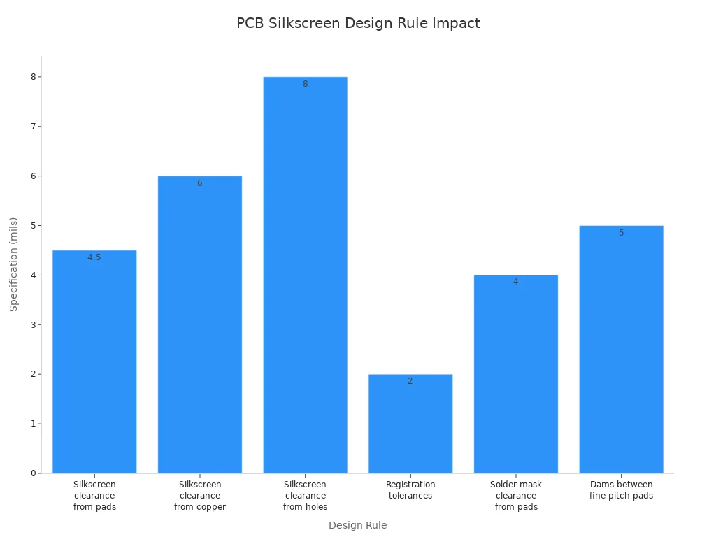
You can stop common silkscreen mistakes by following simple rules. Use a checklist in your pcb design steps. Good habits, like keeping silkscreen away from pads, help you build better boards. Using clear text makes assembly easier. The table shows how these rules help make boards and raise success rates.
Design Rule | Specification | Impact on Manufacturability and Yield |
|---|---|---|
Silkscreen clearance from pads | 4.5 mils | Fewer problems happen when soldering |
Silkscreen clearance from copper | 6 mils | Parts are placed more accurately |
Registration tolerances | 2 mils | Stops mistakes when putting parts together |
Keep learning by checking IPC standards and taking classes like IPC CID or CPCD. When you learn more, your silkscreen designs get even better.
FAQ
What is the main purpose of silkscreen on a pcb?
You use silkscreen to add labels, symbols, and outlines. These markings help you identify components and guide assembly. Clear silkscreen makes your work faster and reduces mistakes.
How do you choose the right font size for silkscreen?
You should select a font size that is easy to read. Most manufacturers recommend at least 1.0 mm height. Always check your manufacturer’s guidelines before you finish your design.
Can you put silkscreen over pads or vias?
No, you should never place silkscreen over pads or vias. This can cause soldering problems and may lead to poor connections or defects during assembly.
What color works best for silkscreen markings?
White silkscreen works best on dark solder masks. If your board uses a light solder mask, you should use black. Always choose a color that stands out for easy reading.
How do you check for silkscreen errors before manufacturing?
You can use your design software’s built-in checks. Review your Gerber files carefully. Look for overlaps, missing labels, or unclear text. This step helps you avoid costly mistakes.
See Also
Addressing Issues and Solutions in SMT PCB Design
Essential Considerations When Designing PCB Circuit Boards
Effective Strategies for Quality Control in PCB Production
Key Insights for Designing Multi-Layer PCB Layouts
Ten Strategies to Reduce Expenses in Custom PCB Manufacturing