Essential Technical Points for AI Accelerator PCB Design

You will face many special problems with ai accelerator pcb design. High-speed signals need special materials in every printed circuit board. You must handle complex stack-up and make sure layers line up exactly. The table below lists some common problems you may see in ai hardware and pcb making. You need to pay close attention to signal integrity, power delivery, heat issues, and reliability. This helps all parts in your design work their best.
Challenge Type | Details |
|---|---|
High Layer Count Structure | Multilayer stacking with tight alignment tolerances (<5 μm) stops signal reflection problems. |
High-Frequency, High-Speed | Dielectric materials must keep Df < 0.002 at 10 GHz to lower signal loss. |
HDI and Microvias | Advanced via technology and laser drilling allow over 5,000 microvias per square inch. |
Thermal Management | CTE must match copper so delamination does not happen during soldering. |
Key Takeaways
Make sure signals stay strong by controlling impedance. Match the lengths of traces and stop crosstalk. This keeps fast signals clear and dependable.
Build strong power networks with bulk and bypass capacitors. Put capacitors near ICs to keep power steady and stop voltage drops.
Use good EMI and EMC plans like shielding, grounding, and smart layout. This keeps signals safe from noise and follows the rules.
Pick high-speed materials with low loss tangents for your PCB. This helps signals work better and lets data move fast.
Do careful stress tests and plan for the product’s life. Use things like thermal cycling and environmental checks to find problems early.
Signal Integrity in AI Accelerator PCB Design
Keeping signal integrity is very important in ai accelerator PCBs. High-speed signals can lose quality if you do not use careful design rules. You need to watch impedance control, length matching, and crosstalk mitigation. These steps help your ai hardware work well.
Impedance Control
You must control impedance to stop problems in high-speed circuits. If impedance does not match, signals can bounce back and cause mistakes. This can make your data bad and even break your circuit. Here are some common issues when impedance is not controlled:
Reflections go up and cause signal loss.
Signal quality gets worse, which is bad for high-speed digital circuits.
Mismatched impedance makes signal transmission and circuit work poorly.
You should always check trace width, spacing, and layer stack-up to keep impedance steady. High aspect ratio and tight pattern alignment make this step harder in ai accelerator designs.
Length Matching
Length matching is important for high-speed differential pairs. If trace lengths do not match, signals can arrive at different times. This causes timing mistakes and hurts signal integrity. You need to follow strict tolerances for different data rates. The table below shows the recommended length matching tolerances:
Data Rate | Recommended Length Matching Tolerance |
|---|---|
Low-speed signals (below 1 Gbps) | ±10 mils (0.254 mm) |
High-speed signals (1 Gbps and above) | ±5 mils (0.127 mm) or ±2 mils (0.050 mm) depending on protocol requirements |
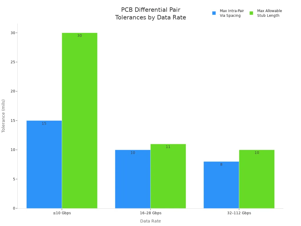
You can see how tolerances get tighter as speeds go up in the chart below:
Crosstalk Mitigation
Crosstalk happens when signals from one trace mess up another. This is a big risk in high-speed ai hardware. You can lower crosstalk by keeping enough space between traces and using ground planes. Careful routing and shielding also help. Always check your layout for tight spots where signals might jump between traces. Good crosstalk control keeps your signal integrity strong and your design reliable.
Power Distribution for AI Accelerator PCBs
You need strong power networks in ai accelerator pcb design. Power integrity is important for every ai hardware project. If you do not plan power paths, parts can stop working or slow down.
PDN Design
You should use good steps for power networks. Use bulk capacitors for low-frequency needs. Put bypass capacitors close to IC power pins for many frequencies. Keep power paths short and use ground planes that do not break. Add enough vias to help current move and keep power strong. Always run PDN tests before you make the board. These steps help you find problems with impedance, voltage drop, and ripple early.
Tip: Put bypass capacitors close to ICs. This lowers loop inductance and makes power better.
Decoupling Placement
You must pick the right capacitors for each frequency. The table below shows how to choose and put capacitors on your pcb:
Tier | Frequency Range | Capacitor Type | Purpose |
|---|---|---|---|
Tier 1 | 10kHz - 1MHz | 100-470uF polymer aluminum or tantalum | Handle low-frequency load steps |
Tier 2 | 100kHz - 10MHz | 10-100uF X5R or X7R MLCC | Supply charge during transient events |
Tier 3 | 1MHz - 100MHz | 10nF-1uF X7R MLCC | Suppress high-frequency resonances |
You should put capacitors as close as you can to the power pins of your ai hardware. This keeps power networks steady and protects signal quality.
Power Layer Layout
You need to make your power layer layout better to lower voltage drop. The table below lists ways to do this for your pcb:
Strategy | Description |
|---|---|
Voltage Regulator Placement | Put voltage regulators close to AI chip power pins to lower trace resistance and inductance, which cuts voltage drop |
Power Plane Impedance | Use thick copper layers and keep power and ground planes close to lower impedance and help current flow |
Multi-phase Regulation | Put more regulators around high power parts to share current and lower heat stress |
You must keep voltage regulators near the GPU or AI chip. Put output inductors 15-25mm from the package edge. This helps fast power changes and keeps power strong. If you do these things, your ai accelerator pcb design will work well for all parts.
EMI/EMC in PCB Design
EMI and EMC are very important in AI accelerator PCB projects. You need to protect your circuits from outside noise. You also need to keep your signals clean. If you do not care about EMI and EMC, your board may not work right. It could fail tests or lose data. You can use smart ways to lower interference and keep signals strong.
Shielding and Grounding
There are many ways to lower EMI in your PCB. These ways help keep your signals safe:
Leave enough space between traces to stop unwanted coupling.
Use differential signaling for fast paths.
Put guard traces next to sensitive lines.
Make trace impedance stable for good signals.
Use electromagnetic absorbing materials and coatings.
Build strong grounding like ground planes and via arrays.
Use shielding covers and enclosures outside the board.
Plan signal routing and layout carefully.
Tip: Put ground planes under important signal layers. This lowers EMI and helps your board pass EMC tests.
Noise Reduction Layout
You can lower noise by making smart layout choices. Keep noisy parts away from sensitive circuits. Route fast signals on inner layers between ground planes. Use short traces and do not use sharp corners. Group similar signals together. You can use via arrays to connect ground layers and block noise paths.
Layout Strategy | Effect on EMI/EMC |
|---|---|
Short traces | Less radiated noise |
Inner layer routing | Better shielding |
Via arrays | Stronger ground connection |
Grouped signals | Lower crosstalk |
Regulatory Testing
You must test your PCB for EMI and EMC before selling it. Use test labs to check if your board meets FCC, CE, or other rules. Add test points and connectors to help with testing. Check your design and fix weak spots. If your board passes, you can sell it with confidence. If it fails, you need to improve shielding, grounding, or layout.
These steps help your AI accelerator PCB meet all rules and keep signals strong.
PCB Materials for AI Accelerator Performance
High-Speed Material Selection
You need to pick the right materials for your pcb when using high-speed signals. The material you choose can change how well your board moves fast data. Many engineers use special laminates to keep signal loss low. The table below lists some high-speed materials and their loss tangent values. A lower loss tangent means less signal loss, which is better for your design.
Material | Loss Tangent (Df) | Application |
|---|---|---|
Rogers RO3003 | < 0.002 | High-speed applications |
Panasonic Megtron 7/8 | < 0.002 | High-speed applications |
ITEQ IT-988GSE | < 0.002 | High-speed applications |
You should use these materials if you want your pcb to handle fast data and advanced parts.
Dielectric Properties
The dielectric properties of your pcb material affect how fast signals move and how much energy they lose. A lower dielectric constant lets signals travel faster, which is important for high-speed circuits. If you use a material with a low dissipation factor, you keep signal loss small. This helps your signals stay strong, even over long distances. You need to check both dielectric constant and dissipation factor when you pick materials for your pcb.
Note: Low dielectric constant and dissipation factor help your high-speed signals stay clean and fast.
Cost vs. Performance
You must think about both cost and performance when you pick materials for your pcb. Advanced substrate-like pcbs give you better data transfer and signal quality. These materials also help with heat control, which is important for high-speed systems. You may see trade-offs in copper surface types. Rough copper can cause more signal loss, but smooth copper may not stick as well. You need to find a balance between low loss and strong sticking.
Here is a table that compares traditional and advanced pcb processes:
Aspect | Traditional PCB (Subtractive) | mSAP (Modified Semi-Additive Process) |
|---|---|---|
Line/Space | 30μm/30μm | 10μm/10μm (volume) |
Impedance Control | ±15% | ±5% |
Microvia Pitch | 100μm+ | 50μm |
Peel Strength | >4 N/cm | 6–8 N/cm (with treatment) |
Cost Implication | Higher due to inefficiencies | Lower with optimized processes |
You should look at both the technical needs and the budget for your project. This helps you make the best choice for your pcb and all its parts.
Advanced PCB Stack-Up and Construction
High Layer Count Challenges
You face many challenges when you build a pcb with a high layer count. Each layer must line up exactly. Small mistakes can cause big problems in high-speed circuits. You need to keep signal paths stable and manage heat well. The table below shows common challenges in high layer count pcb stack-ups:
Challenge | Description |
|---|---|
Impedance Deviation | Tiny deviations can lead to system failure. You must use millimeter- to micrometer-level precision. |
Signal Integrity | You must prevent noise from corrupting vision data streams in compact designs. |
Thermal Management | You need to handle severe thermal loads from deep learning workloads. |
Power Delivery | Reliable power delivery is needed for high current demands. |
Multi-Layer Pressing
You must press many layers together to build a strong pcb. Each layer must stay flat and not shift. If layers move, you lose signal quality in high-speed circuits. You need to use special pressing methods to keep layers tight. This helps you control impedance and keep signals stable. You also need to watch for air pockets and uneven surfaces. These can cause heat problems and lower performance.
Tip: Use careful pressing steps to keep layers flat and strong. This helps your pcb handle high-speed signals and heavy workloads.
Stack-Up Design
Stack-up design shapes how your pcb works. You must plan each layer for signal paths, power, and heat. Controlled impedance routing keeps signals stable in high-speed circuits. Multilayer pcb designs lower crosstalk and boost power integrity. You can use thermal vias and heavy copper layers to move heat away from hot spots. The list below shows how stack-up design helps your pcb:
Controlled impedance routing keeps high-speed signals stable.
Multilayer pcb designs lower crosstalk and improve power delivery.
Thermal management uses vias and thick copper to move heat.
You need to plan your stack-up design with care. This helps your pcb work well in high-speed ai accelerator systems.
Space Optimization in AI Accelerator PCB Design
You have to use all the space on your pcb. Space optimization lets you add more features. It also keeps high-speed signals strong. Using smart routing methods can make your board work better and last longer.
Multi-Order Blind Via Technology
Multi-order blind via technology helps connect layers without using extra space. You drill tiny holes that only go to certain layers. This keeps the pcb thin and stops signal loss. You can put parts closer together. Routing paths get shorter. Shorter paths mean less resistance and better signals. Many engineers use multi-order blind vias in AI accelerator pcb projects. This saves space and makes routing better.
Tip: Multi-order blind vias make your pcb smaller and routing easier.
Inner Layer Gold Fingers
Inner layer gold fingers help with routing. These connectors are covered with gold over nickel. Gold makes them conduct well and stops rust. You must follow IPC rules for gold thickness. At least 30 µin of gold keeps connections strong. Gold fingers can be used many times and still work well. They give low-resistance connections for fast data.
Gold fingers conduct signals well.
Gold stops rust.
The right thickness keeps connections strong.
IPC says use at least 30 µin for long life.
In one lab, a training server stopped working. The gold fingers wore out after many uses. This caused signal problems. It was a big problem for fast systems like PCIe 5.0. You must check gold finger quality to keep routing good.
Routing Efficiency
Routing efficiency means signals take the shortest path. You need to plan your pcb so signals move fast. Smart routing tools help you avoid crossing paths and lower noise. Group signals that are alike together. Keep power and ground paths short. Good routing lowers heat and makes your board work better. Your pcb will last longer and support AI accelerator hardware well.
Routing Strategy | Benefit |
|---|---|
Short paths | Faster signal transmission |
Grouped signals | Less interference |
Smart layout tools | Fewer crossing paths |
You can get better routing by using these ideas together. Your pcb will work well and be very reliable for AI accelerator hardware.
Parallel Processing and Memory Topology
Memory Routing
You need to plan memory signal paths carefully. This helps your AI accelerator move data fast. Good routing keeps bandwidth high and latency low. Use special thermal materials and heat spreaders. These keep chip temperatures under 85°C. This stops memory chips from getting too hot. You can check signal quality with S-parameter tests and eye diagrams. Jitter budgeting also helps you find weak spots. These tests show if your memory signals are strong. Keep voltage steady within ±3% of the target. Put decoupling capacitors close to memory chips. This helps them handle fast current changes up to 50A. Here are some tips:
Use heat spreaders and airflow to cool chips.
Test signals with eye diagrams and S-parameters.
Place decoupling capacitors near memory chips.
Keep voltage steady for good performance.
HDI Techniques
High-Density Interconnect, or HDI, helps with parallel processing. HDI lets you put parts closer together. It also makes signal paths shorter. You get smaller vias, thinner traces, and more layers. These things lower signal loss and crosstalk. Your data stays clear at high speeds. HDI stackups give some layers just for power delivery. This helps with fast signals and many layers. Using HDI makes your PCB layout better for parallel processing.
Tip: HDI makes signal paths short and lowers interference.
Synchronization
You must keep memory access in sync for good parallel processing. Cache memory stores data close to the processor. This makes access faster and cuts down on wait time. Multi-level cache gives both speed and storage. Shared registers let processors sync without using extra memory. The Cray X-MP used shared registers for fast sync. The Cray T3E used a 3D torus so nodes could talk with low delay. You can use these ideas to help your AI accelerator run smoothly.
Cache memory makes access faster.
Multi-level cache balances speed and storage.
Shared registers help processors sync quickly.
3D torus links give fast communication.
Thermal Management for AI Accelerator PCBs
You have to watch heat control when you design AI accelerator PCBs. High-power chips make a lot of heat. If you do not manage this heat, your board can break or slow down. You need good ways to keep your system safe and working well.
Cooling Solutions
There are many ways to move heat away from your PCB. Each way helps with different jobs and power needs.
Thermal vias and copper coin inserts take heat from hot spots to cooler places.
Phase-change materials soak up sudden heat jumps. These work well when workloads change a lot.
Liquid metal cooling moves heat better than old thermal pastes. You can run AI accelerator chips faster without getting too hot. Intel uses liquid metal cooling in Gaudi2 accelerators. These chips use 600W and stay under 85°C.
Vapor chambers and heat pipes spread heat across the server. They help with high-power jobs.
Cold plates with liquid coolant are needed for cards over 700W. Air cooling cannot handle this much heat.
You must pick the right cooling for your board. This keeps your system steady and protects your parts.
Heat Sink Integration
Using heat sinks, like microchannel types, makes cooling better and more reliable. You can control heat better and lower resistance.
Thermal tests show chiplet-microchannel stacks cool well together. Cooling works better.
Interlayer microchannel cooling gives high efficiency and is flexible. This method solves hard heat problems.
You should use advanced heat sinks to keep your PCB cool. This protects your AI accelerator and keeps heat under control.
Thermal Simulation
You can use thermal simulation tools to check your design and spot heat problems. These tools help you make smart choices and improve your board.
Tool | Capabilities |
|---|---|
Siemens Simcenter Flotherm | Gives accurate heat checks at chip, package, and system levels. |
Calibre | Gives detailed chip analysis for better heat modeling. |
Integration | Mixes measurements and AI to predict heat problems better. |
You should run heat tests early when you design. This helps you find weak spots and pick the best cooling.
Reliability in AI Accelerator PCB Design
You must care about reliability in ai accelerator pcb design. Reliable boards help your systems last longer. They also stop expensive failures. You can do this by using good manufacturing steps. You should test your boards with strong stress tests. Plan for the whole life of your parts.
Manufacturability
You need to design boards so factories can build them easily. This helps make boards with few mistakes. Here are some important things:
Use line widths and spacing under 25 micrometers for better performance.
Keep impedance control within ±5% for high-speed signals.
Make sure your power network has low impedance, less than 5 milliohms.
Add shielding to meet EMI and EMC rules.
Handle high thermal density to stop parts from getting too hot.
Aim for yield rates above 95% for normal boards. Use special steps for complex ai accelerator designs.
Tip: Good manufacturability lowers mistakes during steps like photolithography and etching. This helps you build reliable boards every time.
Stress Testing
You must test your boards to see if they can handle real use. Stress testing finds weak spots before your ai accelerator is used. Try these methods:
Environmental stress screening puts your pcb through temperature changes and humidity to find early failures.
Thermal cycling checks if your board can survive fast temperature swings.
Burn-in testing runs your parts at high temperatures to show hidden problems.
Mechanical stress tests shake or bend your board to check for damage.
These tests help you find problems early and make your pcb design more reliable.
Lifecycle Planning
You need to plan for the whole life of your ai accelerator and its parts. Use these ideas to help your boards last longer:
Strategy | Description |
|---|---|
Optimizing GPU Utilization | Use your GPUs better to need fewer and save energy. |
Advanced Cooling Solutions | Keep your boards cool to stop overheating and make them last longer. |
Robust Design and Manufacturing | Build strong boards that last longer and work well in tough places. |
Note: Good thermal management stops overheating and keeps your system running for years. Always check your design to make sure it meets high-speed and reliability needs.
You now know the main ideas for good AI accelerator pcb design. Make sure you keep signals clear, power steady, and heat under control. Try these steps to make your design better:
Look at your layout to find signal or power problems.
Test your board to see if it gets too hot or breaks.
Pick materials that work best for your project.
Keep learning about new tools and rules. Always make reliability and performance your top goals for every project.
FAQ
What materials work best for high-speed AI accelerator PCBs?
You should pick materials with low loss tangent. They also need stable dielectric properties. Rogers RO3003 and Panasonic Megtron 7/8 are good choices. These materials help signals stay strong and move fast.
How can you improve thermal management in your PCB?
You can use thermal vias to move heat away. Heat sinks and liquid cooling also help cool hot spots. Thermal simulation tools let you check your cooling plan before building your board.
Why is signal integrity important in AI accelerator PCB design?
Signal integrity keeps your data safe and correct. High-speed signals can lose quality if you do not control impedance. You must also match trace lengths and lower crosstalk. Good signal paths help your hardware work better.
What is the role of HDI technology in space optimization?
HDI technology lets you put parts closer together. You use microvias and thin traces for easier routing. This saves space and keeps your PCB small and efficient.
How do you test reliability in your PCB?
You can run stress tests like thermal cycling and environmental screening. Burn-in testing also helps find weak spots. These tests show problems so you can fix them before using your board.
See Also
Essential Design Factors for Reliable HDI PCB Manufacturing
Essential Skills for Mastering Multi-Layer PCB Layout Design
Frequent Challenges and Solutions in PCB SMT Design