Mastering HDI Microvia Design for High-Density Interconnects
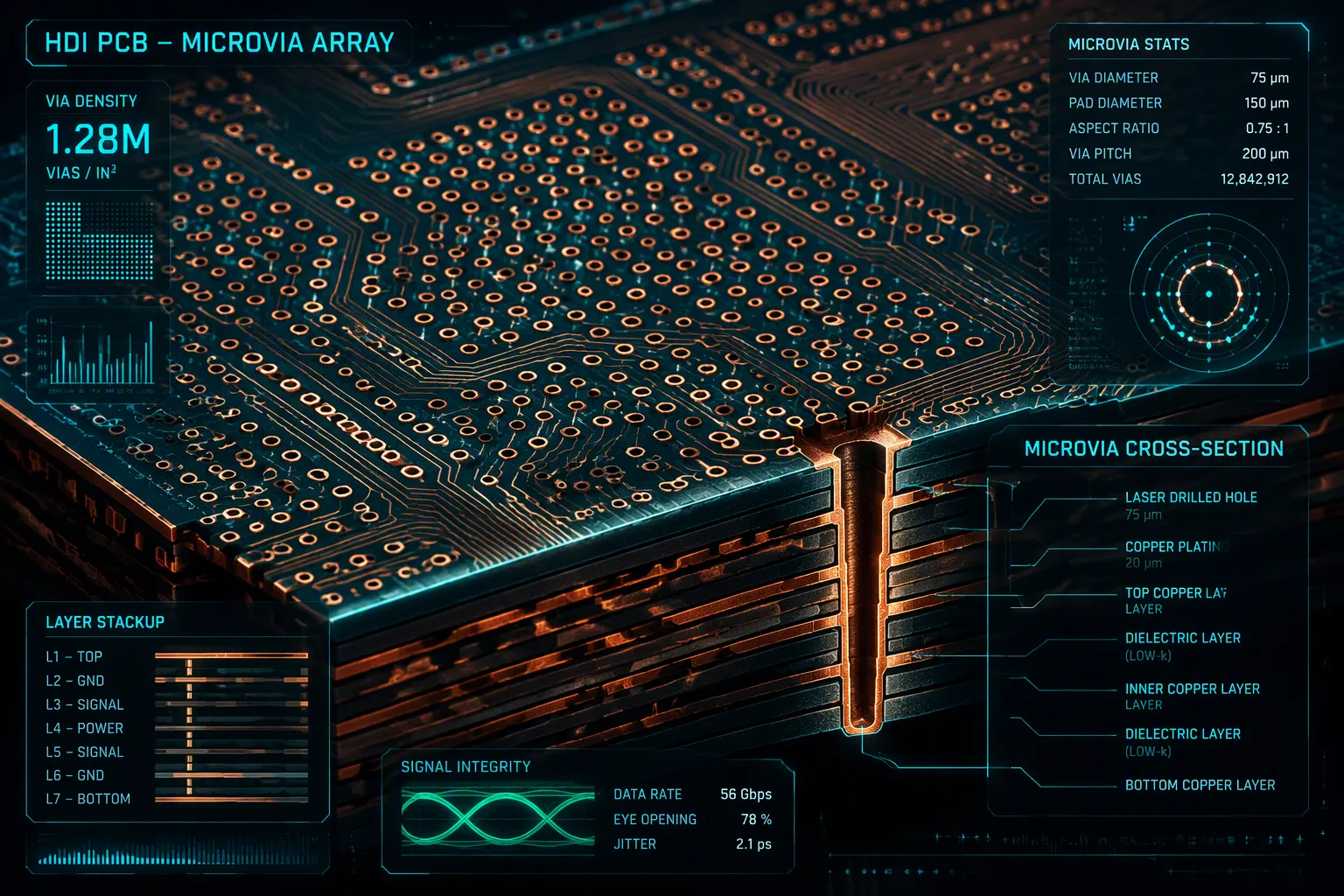
Traditional through-hole vias can't keep up with the density needs of today's electronics. You need a better option for high-density interconnect designs. HDI microvia technology provides that answer. Microvias shrink board size, boost signal integrity, and allow for finer pitch components.
Per IPC-2226, hdi micro-via design needs lines/spaces of 100 μm or less and via diameters of 150 μm or smaller. The table below shows typical production abilities for high density interconnect PCBs.
Parameter | Typical Production | Advanced Production |
|---|---|---|
Min. Line / Spacing | 3/3 mil (~76 μm) | 2.5/2.5 mil (~64 μm) |
Microvia hole size | 100 μm | 75 μm |
Min. drill size | 150 μm | 100 μm |
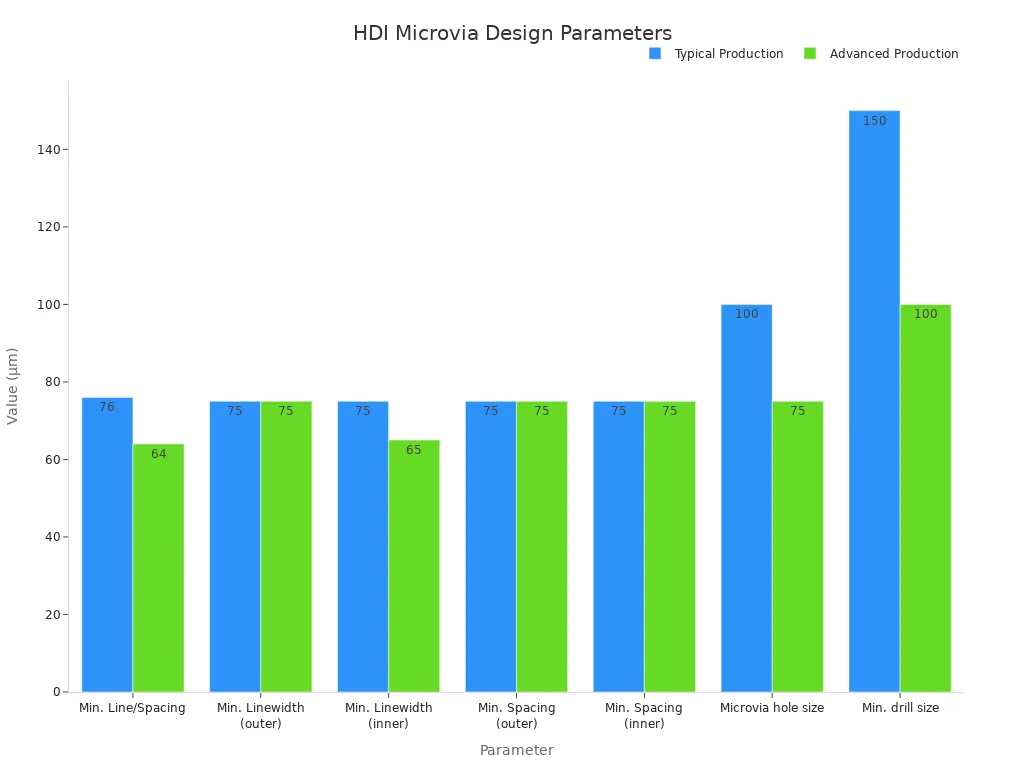
These sizes support high-speed digital systems. You get better signal integrity and high-speed performance through careful design. This technology allows high-speed circuits with dependable interconnect performance on your PCB.
Key Takeaways
Microvias beat through-hole vias for high-density boards. They save space and make signals clearer.
Follow IPC-2226 and IPC-6012E standards. These rules help make microvia design and performance reliable.
Choose copper-filled microvias for better heat and power performance. They manage heat well and work with fine-pitch parts.
Staggered microvias are more dependable than stacked ones. They spread out stress and can handle more temperature changes.
Talk to your manufacturer early. Check design rules and material choices to prevent expensive rework.
The Role of Microvias in HDI PCBs
Microvias are the main support of modern high-density interconnect boards. These small vertical links let you fit more functions into smaller spaces. They also help with finer pitch parts and boost electrical performance. Knowing their role helps you pick better options for your next project.
Why Through-Hole Vias Fall Short
Through-hole vias cause big issues in dense designs. They use up valuable routing space on every layer they go through. This crowding limits your ability to route signals well. The block quote below shows the main problem:
Through-hole vias take up routing space on all layers, creating congestion in the PCB layout.
Electrically, through-hole vias work poorly at high frequencies. They add about 1-2 pF of capacitance, which hurts signal quality. Their size ranges from 0.2 mm to 1.0 mm or more, wasting precious board area. These vias also create stubs—unused parts of the barrel that cause signal reflections.
The stub effect gets worse as frequencies rise. On a 12-layer 25 Gbps networking board, via stubs averaging 0.6 mm caused too much jitter and PCIe compliance failure. After back-drilling cut stubs below 0.15 mm, eye height improved by about 40%. Return loss improved from –12 dB to –22 dB at 5 GHz. Insertion loss improved from –3.5 dB to –1.8 dB. Peak-to-peak jitter dropped from 18 ps to 9 ps. These numbers show why through-hole vias cannot support high-speed digital systems.
Types of Microvias: Blind, Buried, and Stacked
You have several microvia structures to pick from, each with its own benefits. Blind vias connect an outer layer to one or more inner layers. They do not go through the whole board. Buried vias connect inner layers only, staying hidden from the outside. Stacked microvias line up vertically, making direct connections through multiple layers.
Via Type | Structural Difference | Typical Applications |
|---|---|---|
Blind Via | Connects outer layer to inner layers | Communication devices, compact electronics |
Buried Via | Connects inner layers only | HDI boards, medical devices |
Stacked Microvia | Vertically aligned laser-drilled vias | Smartphones, AI hardware, IC substrates |
Stacked microvias give great routing solutions for next-generation uses. They remove through-hole stubs completely, improving impedance control. Staggered microvias offset each layer's via, spreading mechanical stress over a wider area. Research shows staggered setups survive up to 30% more thermal cycles than stacked ones.
Your choice of microvia structures directly affects reliability. Stacked vias focus stress at one point, needing thicker plating of 20-25 µm per IPC-6012 Class 3. Blind vias face thermal stress issues that require careful controlled-depth drilling. Buried vias make inspection harder since you cannot see them from outside.
This design flexibility lets you improve for signal integrity challenges or manufacturing limits. HDI microvia technology enables high-speed circuits with reliable interconnect performance. Mastering these options helps you handle tough applications with confidence.
HDI Micro-Via Design Standards
Three HDI design types shape your manufacturing choices. MICROVIA.hdi works for standard boards with 75/75 μm line/space and 300 μm via pads. SLIM.hdi uses finer features: 50/50 μm line/space and 250 μm via pads. ADVANCED.hdi reaches production limits with 40/40 μm line/space and 200 μm via pads. Your choice among these types directly affects cost, yield, and reliability.
Design Variant | Line/Space | Via Pad Diameter |
|---|---|---|
MICROVIA.hdi | 75/75 μm | 300 μm |
SLIM.hdi | 50/50 μm | 250 μm |
ADVANCED.hdi | 40/40 μm | 200 μm |
IPC-2226 Aspect Ratio and Depth Limits
IPC-2226 sets strict rules for microvia shape. The maximum aspect ratio is 1:1, found by dividing depth by diameter. A 75 μm dielectric with a 100 μm via gives a ratio of 0.75:1, well within limits. The standard also caps microvia depth at 0.25 mm for reliable production.
Lower aspect ratios lower stress buildup. A ratio of 0.25 spreads the load well. Higher ratios near 0.75 raise void and fatigue risks. For practical guidance, a 0.08 mm diameter microvia should be at most 0.16 mm deep. A 0.12 mm diameter microvia can safely go to 0.24 mm deep. The recommended maximum ratio is 2:1, but ratios above this cause uneven plating and cracks during thermal cycling.
Camera alignment tools must keep a tight ±10 µm position match to meet IPC-2226 standards. Proper positioning protects stacked and staggered microvias from full connection breaks, protecting product lifetime.
IPC-6012E Performance Requirements
IPC-6012E defines performance classes for your microvia design. Class 2 and Class 3 have different copper plating thickness and fill quality.
Feature | Class 2 | Class 3 |
|---|---|---|
Copper plating thickness (average) | 20 µm | 25 µm |
Copper plating thickness (minimum in hole) | 15 µm | 15 µm typical |
Via fill percentage (Type VI and VII) | ≥ 75% | ≥ 75% |
Z-axis thermal expansion must stay below 70 ppm/°C. A 40% increase from 50 to 70 ppm/°C can cut lifespan by 95%. Reflow heat tolerance is 260°C peak. Dielectric material must match copper's CTE to reduce thermomechanical stress. Low-loss laminates improve reliability. Staggered microvias are more robust than stacked ones, especially for three or more layers. These standards guide your hdi microvia design for dependable interconnect performance. Following them helps your pcb survive thermal cycling and deliver consistent performance over its life. This hdi microvia technology enables high-density interconnects with confidence.
Design Rules for HDI Microvia Reliability
A reliable board starts with three core elements: aspect ratio, via fill, and layer stack-up. Each one affects how your pcb handles heat and mechanical stress. Get these right, and your board will last.
Aspect Ratio, Via Fill, and Layer Stack-Up
Aspect ratio is the depth of a microvia divided by its diameter. IPC-2226 suggests a ratio of 0.75:1 or less for steady copper plating and stacking. For high-reliability jobs, a ratio of 0.8:1 or less is best. Higher ratios raise the chance of uneven plating and barrel cracks. The formula is simple: aspect ratio equals dielectric thickness plus copper foil thickness divided by microvia diameter. A typical microvia has a diameter of 75-150 µm. The maximum ratio for laser-drilled microvias is about 1:1. Past that, you face reliability issues.
Via fill material matters too. Copper fill gives the best thermal and electrical performance. It offers thermal conductivity of 8 W/m·K, which is over 25 times better than air-filled vias. Epoxy fill costs less and works well for signal vias. Conductive paste sits in the middle. For stacked microvias, you must fill and flatten each via before drilling the next one on top. Copper filling is recommended for bottom-most vias in stacks to stop keyholing from spreading.
Layer stack-up affects mechanical stress and thermal expansion. A balanced stackup around the centerline prevents warpage-induced stress. Use low-CTE materials below 15 ppm/°C to reduce stress on microvias during thermal cycles. Most manufacturers suggest stacking up to 3-4 microvias in a column. Past this, alignment tolerances and thermal stress get hard to manage. Capture pads should be 250-350 µm in diameter for a 100-150 µm via. Account for layer-to-layer registration errors. Always confirm aspect ratio limits, minimum via diameter, and maximum stack count with your fabricator early on. Early fabrication consultation prevents costly redesigns.
Thermal and Reliability Considerations
Thermal cycling puts microvias under heavy stress. Stacked via arrangements focus axial stress at via interfaces. Staggered microvias spread loads stepwise. Under thermal shock from -65°C to 125°C, staggered microvias survive 400+ cycles with almost zero failures. Directly stacked vias show alarming failure rates under the same strain. The reliability risk grows with stack height due to more manufactured interfaces, more cumulative thermal exposure, and more registration variation. These microvias must endure repeated thermal stress.
Copper-filled microvias improve thermal behavior significantly. They reduce junction temperature by 10-20°C in power ICs with thermal via arrays. They also provide 30-50% higher mechanical strength for pad pull than unfilled vias. For via-in-pad layouts supporting advanced BGA packages, copper fill delivers assembly yield above 98% with consistent solder joint volume. Fine-pitch BGA support at 0.4 mm pitch becomes possible. Signal path inductance drops by up to 30%.
Failure modes to watch for include neck fracture, interface failure, void-induced failure, and pad lift. Neck fracture occurs at the top or bottom of the via barrel due to stress concentration. Use a low aspect ratio of 0.75:1 or less and ensure uniform plating thickness of at least 15 µm. Interface failure happens between directly stacked vias due to differential expansion. Limit stack height to 2 vias and use copper filling. Pulsed plating helps achieve void-free filling in these microvias. Void-induced failure comes from voids in plating. Use pulsed plating and optimize parameters. Pad lift results from poor adhesion. Ensure proper cleaning and adhere to minimum annular ring rules.
For demanding applications like automotive or aerospace, boards endure thermal cycles from -55°C to 125°C. Directly stacked via failure rates spike significantly under these conditions. Staggered configurations remain the safer choice. Use simulation tools to predict thermal stress effects. Run a representative D-coupon that reproduces the actual via stackup and manufacturing sequence. Use resistance monitoring during thermal cycling to identify latent opens.
These rules help you master hdi micro-via design for reliable routing behavior. Understanding microvia structures and their thermal behavior ensures your pcb survives tough conditions. This hdi microvia technology enables high-density interconnect boards.
Manufacturing Process for HDI Microvia Technology
You need precise control of laser drilling and plating for microvias. Each variable affects the final quality of microvias. The process directly impacts your pcb's reliability.
Laser Drilling and Plating Techniques
You have two main laser options for drilling microvias. CO2 lasers use thermal decomposition at 9.3–10.6 µm wavelength. They remove organic dielectrics but require prior copper removal. UV lasers use photochemical cold ablation at 355 nm. They can directly ablate copper. The table below shows the key differences.
Attribute | CO2 Laser | UV Laser |
|---|---|---|
Ablation mechanism | Thermal decomposition | Photochemical cold ablation |
Copper handling | Requires prior removal | Directly ablates copper |
Via wall shape | Characteristic taper | Straighter sidewalls |
Heat-affected zone | Larger | Smaller |
Several parameters affect your drilling quality. Pulse energy must balance speed and cleanliness. Higher energy removes material faster but risks debris. Pulse duration from 10 to 50 ns reduces heat buildup. Spot size between 20 and 50 µm prevents oversized holes. Repetition rate from 50 to 100 kHz balances speed and control. The aspect ratio is a critical factor in microvia fabrication. An ideal ratio of 1:1 or lower ensures uniform copper plating. Ratios above 1.2:1 can lead to incomplete plating at the via bottom. For advanced hdi fabrication, you must use thin dielectric layers under 0.1 mm.
You also need to optimize material selection. Prepreg glass style matters. Heavy glass weave scatters the laser beam. Use 1080 or 2116 glass styles. Avoid 7628. Dielectric thickness should stay between 75 and 100 µm. Use 0.5 oz copper for microvia layers.
After drilling, you need a reliable plating process for microvias. It follows three main steps. First, electroless plating deposits a thin conductive layer on the microvia walls. Second, graphic electroplating thickens the copper walls. Third, periodic pulse reverse (PPR) plating completes the filling. Reverse current pulses promote ion replenishment and suppress dendrite formation. You must monitor bath chemistry, temperature, and agitation.
Statistical process control (SPC) helps maintain quality of microvias. You should monitor microvia diameter, capture pad size, depth uniformity, and plating quality. Real-time monitoring of via diameter and depth variation allows early defect detection.
Implementing SPC on laser drilling lines reduced microvia misregistration by 50% in a high-volume HDI production line.
Sequential Lamination and Material Selection
Sequential lamination builds your HDI board layer by layer. Each cycle applies heat and pressure. You must select materials that withstand repeated thermal exposure.
Key material properties determine your success with microvias. The table below shows recommended values.
Property | Recommended Value | Purpose |
|---|---|---|
Glass Transition Temperature (Tg) | ≥ 170°C | Withstands repeated thermal cycles |
CTE (Z-axis) | < 15 ppm/°C | Minimizes stress on microvias |
Dielectric Constant (Dk) | 3.0 – 4.0 | Maintains signal speed |
Dissipation Factor (Df) | < 0.01 | Reduces signal loss |
Moisture Absorption | < 0.5% | Prevents swelling |
High-Tg laminates delay rapid Z-axis expansion. Low-CTE laminates reduce strain differential in stacked microvias. The CTE mismatch between copper and resin is significant. Glass reinforcement has CTE of 6 ppm/°C. Copper has 17 ppm/°C. Resin has about 100 ppm/°C. Below Tg, resin expands 4.5 to 5 times faster than copper. Above Tg, resin expands 17 to 20 times faster. This pressure can cause delamination around microvias.
For advanced hdi fabrication, choose dielectric with Tg ≥ 180°C and low Z-axis expansion. Use lower resin content in some areas to reduce Z-axis expansion. Use high resin content in dielectrics to spread stress. Fine glass weave supports clean vias without fiber pullout. These choices enable advanced pcb manufacturing.
Microvia fabrication requires careful planning across all these factors. Understanding this technology helps you succeed. Your knowledge of laser drilling, plating, and material selection determines your pcb's reliability. This hdi microvia technology enables high-density interconnect design with confidence.
Successful hdi micro-via design requires following IPC standards closely, choosing the right via fill, and knowing what manufacturing can do. You must pick between MICROVIA.hdi, SLIM.hdi, and ADVANCED.hdi based on how dense your board needs to be. Copper-filled microvias allow high density interconnect performance and support via-in-pad for advanced BGA packages.
Real-world use shows stacked and staggered microvias cut board size by 30–50% while boosting signal performance. Staggered setups spread stress better and are easier to make. Even with a 20–100% higher fabrication cost, the benefits win out because you need fewer layers and smaller boards. These microvias are key for reliable routing.
Future hdi microvia technology trends include flexible substrates, picosecond lasers for sub-100µm features, and AI-assisted design tools. Learning these basics gets you ready for next-generation, ultra-thin, high-speed pcb designs. This technology delivers reliable interconnect solutions for demanding pcb applications.
FAQ
What is the maximum aspect ratio for a reliable microvia?
IPC-2226 says the maximum aspect ratio is 1:1 for reliable production. To find this, divide depth by diameter. A 75 μm dielectric with a 100 μm via gives a 0.75:1 ratio. For high-reliability jobs, keep it at or below 0.8:1.
Should you choose copper-filled or epoxy-filled microvias?
Copper-filled microvias give better thermal and electrical performance. They have thermal conductivity of 8 W/m·K, which is over 25 times better than air-filled ones. Epoxy fill is cheaper and works fine for signal vias. For stacked setups, copper filling stops keyholing from spreading.
How do stacked and staggered microvias compare in reliability?
Staggered microvias spread mechanical stress over a larger area. They handle up to 30% more thermal cycles than stacked ones. Under thermal shock from -65°C to 125°C, staggered designs pass 400+ cycles with almost no failures. Directly stacked vias fail more often under the same conditions.
What design variant should you pick for your pcb?
Your pick depends on how dense your board needs to be. MICROVIA.hdi handles 75/75 μm line/space with 300 μm via pads. SLIM.hdi uses 50/50 μm features with 250 μm pads. ADVANCED.hdi reaches 40/40 μm with 200 μm pads. Each step up makes fabrication harder and costs more.
Does hdi microvia technology cost more than standard pcb fabrication?
Yes, expect a 20–100% higher fabrication cost than conventional boards. But you save money in other ways. HDI boards need fewer layers and take up less space. These savings often make up for the higher initial cost, especially for high-density interconnect designs.
See Also
Essential Design Factors For Reliable High-Density Interconnect PCB Production
Analyzing Costs And Benefits Of Stacked Staggered Microvia HDI PCBs
Explore Novel HDI PCB Prototype Techniques Right Now
Understanding The Design And Fabrication Of HDI Any Layer Boards
Advantages Of Using LDI Exposure Machines For HDI PCB Circuits
