HDI PCB Laser Drilling Alignment Strategy: Complete 2026 Guide
You get exact microvias alignment in high-density interconnect building by using live camera systems. Smart laser drilling tools use visual markers and vision calibration to hit registration accuracy of ±10 µm or higher. This automatic step guards your hdi pcb design from a ±0.075 mm drilling positioning tolerance and about ±0.1 mm graphic expansion across inner layers. UV and CO2 laser beams burn 25–75 µm microvia diameters straight into the base material. You need to keep a 0.15 mm minimum clearance distance during the hdi manufacturing process to stop pad breakout. New laser drilling technology manages material warping while meeting IPC compliance standards for each hdi board. Learning this hdi technology improves overall hdi pcb performance and hdi quality.
Key Takeaways
Clever camera systems help laser drills hit target pads with great accuracy.
Right-sized capture pads stop the drill from breaking out when workers make HDI boards.
UV lasers drill tiny microvias, while CO2 lasers make larger holes.
Evenly built board layers lower material bending from heat and pressure during manufacturing.
IPC standards ensure high quality and prevent holes from going outside the metal pads on finished circuit boards.
Precision Laser Drilling Alignment in HDI PCB Design
Careful planning of your high-density interconnect layout guarantees strong electrical results. Good hdi pcb design habits shield the board when materials shift during manufacturing.
Microvia Target Sizing and Annular Ring Calculation
Every hdi pcb design needs correctly sized capture pads to avoid drill breakout. Adding 100 µm to the target via diameter gives the correct capture pad size. That math leaves a 50 µm annular ring along all sides. A correctly sized pad absorbs the ±0.075 mm laser drill positioning tolerance. It also handles the ±0.1 mm graphic expansion that happens while processing inner layers.
Laser type | Minimum via diameter | Annular ring per side | Minimum capture pad diameter |
|---|---|---|---|
UV | 25 µm | 50 µm | 125 µm |
CO2 | 75 µm | 50 µm | 175 µm |
Pick your laser beam source according to the target hole sizes. UV laser tools drill small microvias down to 25 µm. CO2 laser tools handle larger microvias from 75 µm upward. Using correct laser drilling settings ensures microvias make clean contact with pads. Maintain a 0.15 mm minimum clearance distance between copper elements. That gap shields routing tracks from pad edges during circuit board drilling. Clean routing forms strong trace-to-pad joints. It enhances total registration accuracy across all layers.
Layer Registration and Lamination Movement Limits
Controlling material movement is essential throughout the hdi manufacturing process. Heat plus pressure during lamination shift individual layers around. Build a balanced pcb stackup to spread stress evenly across the hdi board. Smart stackup planning reduces heat strain on inner copper layers.
Factories monitor inner layer movement with high-tech tools:
X-ray registration systems check fiducial markers on inner layers following sequential lamination, keeping alignment accuracy within 0.05 mm (~±0.002 inches).
Micro-section analysis checks layer-to-layer alignment and structural microvia quality on finished boards with a 0.15 mm clearance.
Exact layer registration guarantees steady connections between layers. Reliable layer placement stops signal loss inside high-speed routing networks. Precise laser drilling positioning allows you to land on target pads in crowded routing areas. Tight alignment tolerances support these crowded routing zones. A stable stackup maintains solid paths through tricky high aspect ratio vias.
Good laser alignment protects your hdi pcb board against breakout flaws. High-quality registration cuts scrap waste during the hdi manufacturing process. Careful planning simplifies your pcb designing work on complex hdi products. Smart dynamic scaling balances out panel shrinkage right before laser drilling starts. Aligning your hdi pcb design rules with real factory laser drilling limits raises manufacturing yields. This smart plan upgrades your hdi workflow and delivers lasting performance.
Visual Reference Systems for High-Density Board Placement
You require clear target spots to direct modern machinery across your board surface during laser work. Visual placement cameras scan special copper marks before any physical tool hits delicate laminate materials. Proper reference target design ensures exact layer-to-layer placement for each internal layer in complex multi-layer builds. Accurate visual placement prevents costly board waste during board making.
Overall and Nearby Reference Marking Rules
You need to position both overall and nearby reference targets inside your board layout to stop hole-to-pad alignment errors. These visual alignment marks allow high-speed vision cameras to set exact coordinate reference systems across the board before drilling begins.
Mark Category | Size Details | Location Spot | Main Function |
|---|---|---|---|
Global Fiducial | Width | Board edges in an uneven layout | Fixes total panel twisting shift and sideways movement |
Local Fiducial | Width | Close to tight-pin parts | Fixes local board warping and panel stretching |
You must place overall marks in an uneven pattern across diagonally opposite board frame corners. Wide mark spacing reduces angle errors during critical rotation adjustment steps on automated tools. IPC-7351 guidelines suggest keeping an open copper space around every target mark. Make this open area at least 1.5× the target mark width. Never let solder mask coatings cover these bare copper spots.
Include nearby target marks when main vision adjustments fail to fix local material stretching in complex boards. Packed active part layouts need clear visual pathways for high-resolution camera lenses. Thoughtful positioning of parts saves room for local target marks without ruining fast wire routing paths inside crucial signal layers. You shield tight wiring paths when you plan target spots early. Great early planning guards your full wire routing room while keeping clear visual paths during drill setup steps.
Real-Time Resizing and Reference Pattern Identification
Multi-step board making steps push thin copper sheets through high heat cycles and pressure steps. Multi-stage pressing shifts internal copper layers out of place over time. Heat treatment creates heavy material shrinking or stretching across inner board layers. Modern positioning tools use multi-mark array cameras to measure panel shifts continuously on advanced board tools.
You manage total manufacturing build changes through step-by-step target math:
Optical cameras find reference arrays on inner layers to calculate exact side-to-side and up-down size factors before laser light fires.
Computer programs reset laser path targets automatically to match real physical board shrinking across crowded wiring areas.
Visual camera tools check target mark quality constantly to keep strong positioning precision during drill runs.
Modern laser drill tools shift beam locations automatically based on live camera video feeds. Smart laser machines adjust small hole target positions continuously to prevent pad boundary damage. Exact laser beam position adjustments preserve full layer placement accuracy throughout complex multi-step production runs.
You should balance copper weight distribution across your board layout to limit uneven heat stretching. A balanced board layout helps keep material changes fully predictable. Unbalanced board layers twist and stretch unevenly under heavy heat strain. Predictable board movement allows optical cameras to follow placement target groups much faster around tiny target pads during visual drilling. Proper laser drill settings joined with clear reference layout rules keep your total output high and secure strong board quality. Smart board layout choices deliver reliable power performance on every board. Strong board design steps make complex board making simple.
Laser Equipment Mechanics and Real-Time Vision
Modern cameras scan every hdi panel during fast laser drilling runs. Visual sensors read board marks to adjust target spots before the beam fires. Automated systems keep alignment accuracy within ±10 μm. They keep via placement accuracy within ±15 μm of planned layouts. Fast tools perform laser drilling up to 9,000 vias per second across detailed hdi board surfaces. Camera systems shield crowded hdi patterns during ongoing circuit board drilling work.
Laser systems drill thousands of vias per minute with steady accuracy, maintaining fast production speeds while protecting board quality.
Machine optics focus light beams onto clean target spots across every pcb layer:
Beam shaping – Optics adjust the beam shape to control hole sizes from the start.
Focusing and positioning – Computers guide the beam to exact drill spots for tight hdi layouts.
Automated Vision Calibration and Optical Alignment
Smart vision software guides fast optical scanners while drilling microvias. Cameras capture live images to fix panel shifts before laser ablation starts. Automatic alignment shields target pads from hole breakout during laser drilling. Using this advanced technology improves hole placement across every hdi layer.
Your initial hdi pcb design sets clear location targets for the vision scanner. Smart design choices help automated tools find coordinates fast. Advanced hdi boards need steady optics to process tiny microvias correctly. Visual calibration ensures exact hole landing during full laser drilling runs.
Beam Ablation Dynamics and Thermal Deflection
Precise energy controls handle heat generation during beam ablation cycles. A UV laser with a 355 nm wavelength cuts copper using cold ablation. CO2 beams clear dielectric material cleanly while copper pads bounce off extra energy. Matching power levels to material types prevents heat damage in modern hdi manufacturing.
Material | Laser type | Pulse setting | HAZ prevention effect |
|---|---|---|---|
Rogers laminate | UV 355 nm | 5–15 W low power | Limits HAZ for dielectric stability |
PTFE substrate | UV 355 nm | 5–10 W short pulses | Prevents soft material melting |
Careful energy control allows safe laser drilling through high aspect ratio vias. Pulsed laser light opens top copper without scorching bottom pads. You shield pcb substrates by matching energy amounts to board layers, essential for hdi production. Proper pulse settings create clean hole walls on every hdi board.
Substrate Distortion and Thermal Lamination Controls
Dielectric Material Shrinkage and Expansion
Heat changes board sizes during the hdi manufacturing process. You must control heat expansion across internal layers to keep trace interconnections safe. Glass fibers expand at ~6 ppm/°C, while resin expands at ~100 ppm/°C. Copper expands at ~17 ppm/°C. Standard FR-4 shifts 10–20 ppm/°C on the X-Y plane and 50–70 ppm/°C along the Z-axis.
Even differences of a few ten-thousandths in the shrinkage rate of different materials can cause microvia misalignment, so matching thermal expansion/shrinkage is critical in HDI lamination.
Unmatched stress makes boards warp during heavy press steps. Shrinking 0.5% on a 100 mm board causes 0.5 mm of bad alignment. A tiny 10 μm layer shift makes computers recalculate to hit exact drill targets across many board layers. You protect your high-density interconnect layout by choosing a balanced pcb stackup. A symmetric stackup balances cooling forces across your whole hdi pcb design.
Copper Foil Profiles and Desmear Optimization
Material choices directly change laser accuracy. Thin copper foils (≤18 μm) help laser beams cut clean microvias into target spots. You simplify your hdi pcb design work by choosing low-profile glass cloths like 1035, 1067, or 1086. These simple materials allow smooth laser beam passes. Steady laser light absorption stops board damage near tight signal routing paths.
Clean holes guarantee strong electrical links across high-speed routing paths. Laser heat leaves tiny debris behind during normal board drilling runs. You use plasma desmear steps to clean out resin smear before starting copper plating. This extra cleaning step opens safe connection paths between inner copper layers. Safe cleaning steps shield tight routing lanes and stop open circuits inside busy routing areas. Careful pcb stackup planning raises output yields during the main hdi manufacturing process. Controlled laser drilling settings and smart hdi design rules deliver strong hdi pcb performance. Exact laser drilling choices protect total pcb quality for every hdi board using modern hdi technology on your hdi layout.
Drilling Quality Inspection and Reliability Standards
Inspect finished board panels to confirm exact hole placement across all hdi structures. Quality assurance teams use strict rules to check laser drilling results on complex high-density interconnect boards.
Microvia Alignment Verification via IPC-2226 and IPC-6012
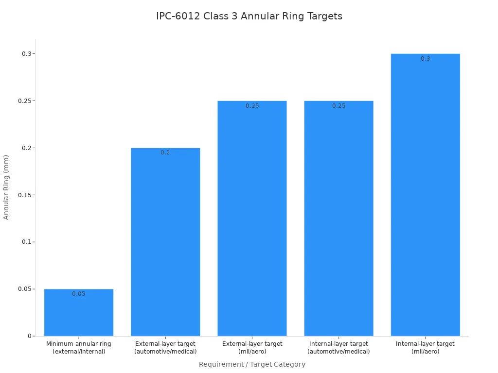
Verify proper microvias placement by using guidelines from IPC-2226 and IPC-6012 standards. Standard IPC-2226 calls for a 25 µm minimum annular ring around laser drilled holes to secure target connections. Industry standards like IPC-6012 Class 3 allow zero breakout on high-reliability boards. Keep proper clearance across internal layers to shield dense signal pathways during high-speed routing steps.
Standard | Inspection Requirement | Target Value |
|---|---|---|
IPC-2226 | Minimum annular ring width | 25 µm |
IPC-6012 Class 3 | Permitted pad breakout | Zero breakout allowed |
IPC-6012 Class 3 | Microvia barrel plating thickness | 12 μm |
Following correct drilling rules protects your hdi pcb design from field failures caused by poor registration accuracy. Designers pick a balanced pcb stackup to prevent severe board warping during production. A stable stackup limits thermal stress across important inner layers during hot processing stages.
Cross-Section Analysis and Breakout Detection
Find hidden internal defects by cutting hdi test coupons for detailed microsection analysis. Optical measurement tools check laser target landing accuracy by measuring hole positions, diameters, and roundness. Optical microscopy at 50X–500X magnification shows internal layer alignment without damaging production hdi panels.
Microsectioning test coupons reveals via-to-pad registration under high magnification, letting inspectors confirm copper coverage before approving full production runs.
Engineers check structural integrity through systematic testing steps:
Technicians mount test coupon cross-sections inside resin blocks for polishing.
Inspectors use optical comparators to verify via depth, copper target exposure, and wall plating.
Software measures remaining annular ring width to confirm zero breakout on internal routing pads.
Careful quality checks improve total laser drilling performance throughout the hdi manufacturing process. Optical tools prove that every laser beam hits target pads accurately. Reliable laser operations maintain clean signal routing channels across all layers. Strict drilling quality controls protect every hdi pcb during the hdi manufacturing process. High quality standards back reliable hdi board performance in tough electronics applications.
Mastering laser registration requires clear strategies for every hdi board. You shield your hdi pcb design by matching physical pad clearances with real-time laser vision tools. Always keep a 0.15 mm clearance distance across all hdi layers. Fast camera tools fix tiny position errors during active laser drilling runs. This dynamic tracking stops hole breakout across dense hdi circuits.
Align physical clearances with live camera compensation to protect every hdi structure.
Apply material expansion offsets to CAM layout files during initial setup. Smart hdi layout adjustments balance heat distortion across each hdi pcb. Modern hdi drilling equipment hits every hdi microvia cleanly, improving overall hdi yield.
FAQ
How do you prevent pad breakout during laser drilling?
Keep at least 0.15 mm of space between parts to avoid breaking pad edges. Good board planning helps absorb small drill movements and material stretching. Clear paths around pads shield them while your board is being made.
What microvia sizes can UV and CO2 laser beams create?
UV lasers cut tiny holes down to 25 µm wide. CO2 laser tools drill larger openings that start at 75 µm. Picking the best laser gives you the right hole size for every board layer.
Why does heat strain affect registration accuracy in hdi manufacturing?
Heat makes plastic layers stretch much faster than glass strands when layers are pressed together. An uneven board layer layout causes uneven stretching across the panel. Smart camera tools calculate these size changes before drilling, keeping holes centered on target pads.
How do vision systems improve alignment on an hdi board?
Quick camera sensors scan special marks on every board panel. Modern machines then guide the laser beam to hit exact target spots. Automated camera checks stop hole placement errors across crowded board layouts.
What standards govern microvia quality on an hdi board?
Check finished boards using IPC-2226 rules to keep a 25 µm ring around holes. Testing teams ensure no holes miss their pads on IPC-6012 Class 3 boards. Careful drill checks protect signal paths on every single board.
See Also
Understanding The Complete Process Of HDI PCB Laser Via Filling
Achieving Flawless Flatness In HDI PCB Plated Laser Vias
Smart Cost Reduction Tactics For HDI PCB Back Drilling Operations
An Essential Guide To Back Drilling In HDI Circuit Boards
Exploring Cutting Edge Techniques For Modern HDI PCB Prototype Fabrication
