How to Perform PCB Slice Testing for Internal Quality
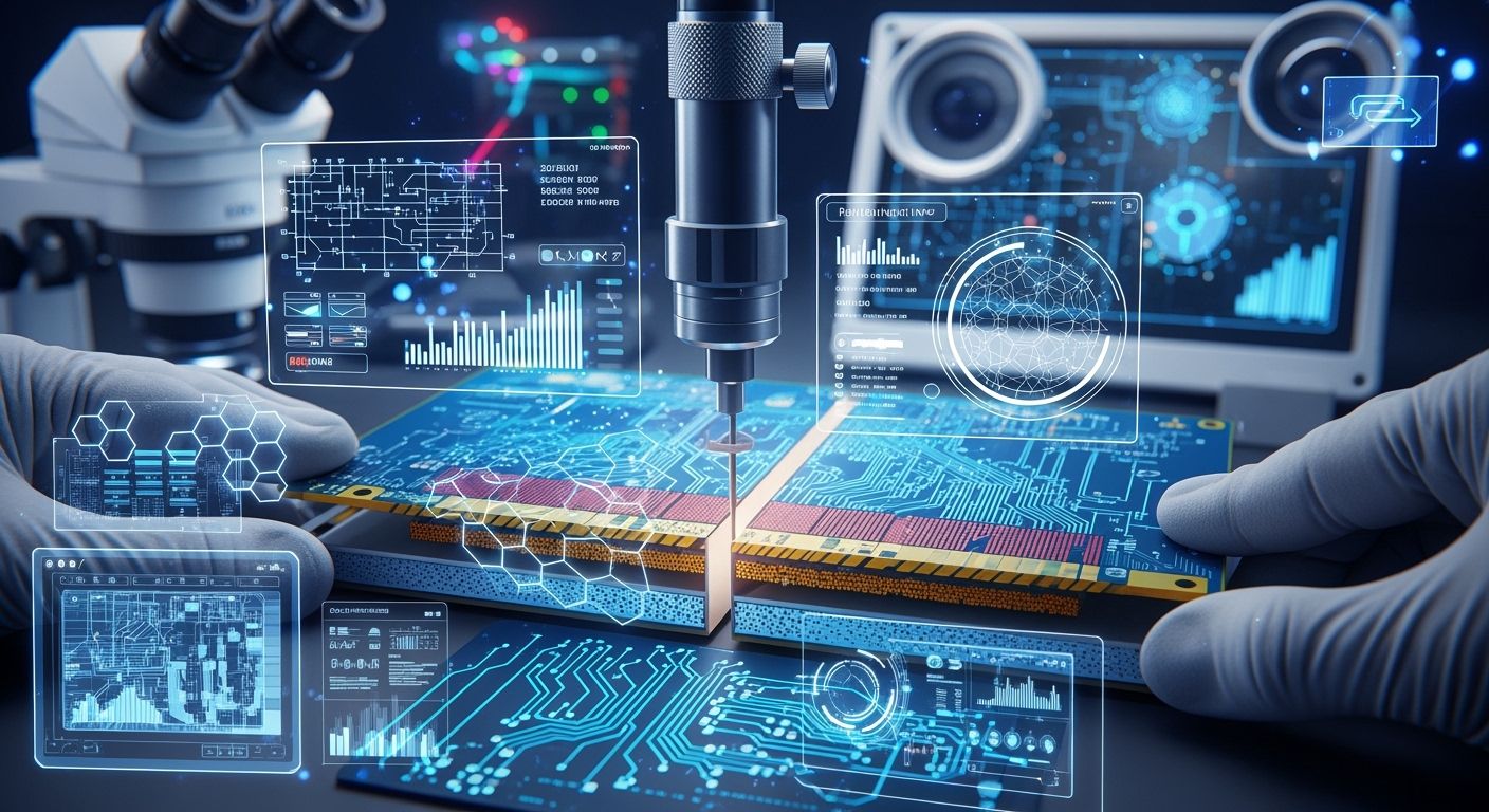
You use pcb slice testing to check the inside of a pcb and reveal hidden issues. This process lets you cut a pcb, prepare a sample, and inspect it closely. You need to understand how to handle the pcb, which tools to use, and how to look for signs of trouble. Careful testing helps you spot problems early and keep the pcb safe and reliable. You improve pcb quality when you follow each step and use the right equipment.
Key Takeaways
PCB slice testing shows hidden problems inside the board. It helps you find issues like cracks and delamination early.
Prepare samples carefully by cutting, grinding, and polishing them. This makes sure you get clear results when you analyze them.
Use the correct tools, like microscopes and X-ray machines. These tools help you check and study the board more accurately.
Follow IPC standards to make quality control better. This lowers mistakes and helps customers trust your work.
Use different testing methods together for a complete check. This helps you find and stop PCB failures.
PCB Slice Testing Overview
What Is PCB Slice Testing
PCB slice testing lets you look inside a pcb. This method shows layers and connections that you cannot see. First, you prepare a sample from the pcb. You cut the sample and polish it. Sometimes, you corrode the sample to see the cross-section. You use different tools to check and study the sample. These tools include microscopes, scanning acoustic microscopes, and infrared analysis systems. Each tool helps you see something special about the pcb’s parts and materials.
Here is a table that lists common ways to analyze pcb slice testing:
Analytical Technique | Description |
|---|---|
Slice analysis | You get the cross-section of pcb by sampling, slicing, polishing, and looking at it. |
Scanning acoustic microscope | You find inside defects like cracks and delamination with high-frequency sound waves. |
Microinfrared analysis | You check what materials are made of by seeing how they absorb infrared light. |
Scanning electron microscope analysis | You look at tiny structures and surfaces using high magnification. |
Differential scanning calorimeter | You study heat properties by measuring power changes as temperature goes up or down. |
Thermomechanical analyzer | You check how materials act when heated or pushed. |
Thermogravimetric analyzer | You measure how much a substance weighs as temperature changes to learn about its heat stability. |
Importance for PCB Quality
PCB slice testing helps you make sure the pcb is good. This process finds defects that can hurt how the board works. You can see problems like cracks, delamination, and bad connections. You use checking and studying to see if the pcb meets rules. You make the pcb more reliable by finding problems early. Testing also helps you fix boards and stop future issues. When you follow the right steps, you keep the pcb safe and high quality.
Tip: If you prepare samples carefully and analyze them well, you get good results from pcb slice testing.
PCB slice testing is important for checking quality. You use checking, testing, and studying to protect the pcb and make sure it works right.
PCB Slice Testing Process
Sample Preparation Steps
You begin pcb slice testing by getting the sample ready. This step matters because you want to see inside the pcb and check its quality. You follow a method to get a clear cross-section for slice analysis. Here are the steps you use:
Sectioning: You cut the pcb to show the cross-section. You try not to damage it so you can see inside clearly.
Mounting: You protect small parts and keep the edges strong. You use mounting to hold the sample for analysis.
Grinding: You fix damage from cutting and make the surface smooth. You use grinding to get the pcb ready for polishing.
Controlled Removal Polishing: You polish the surface and watch how much you remove. You want to keep the inside visible for slice analysis.
Final Polishing: You polish until the surface shines like a mirror. You need this finish for close inspection and analysis.
Tip: If you prepare samples carefully, you get good results in pcb slice testing. You avoid mistakes and make your inspection better.
Slicing, Mosaic, and Polishing
You use slicing, mosaic, and polishing to see inside the pcb. Each method helps you find different parts and defects during slice analysis. You need to follow the steps to keep the pcb safe and get good results.
Slicing: You cut the pcb into thin slices. You use a method that keeps the layers and connections together. You want to see inside for analysis and inspection.
Mosaic: You put the slice in a resin block. You use mosaic to protect the edges and make the sample easy to handle. You keep the inside safe for slice analysis.
Polishing: You polish the slice until it shines. You use polishing to remove scratches and make the surface smooth. You need a clear surface for inspection and analysis.
Here is a table that shows common mistakes during slicing, mosaic, and polishing, and how you can fix them:
Common Errors | Solutions |
|---|---|
Non-manifold edges | Use tools like Netfabb or Meshmixer to fix models. |
Improper model orientation | Put flat surfaces on the build surface and reduce overhangs to make prints better. |
Inadequate support structures | Turn on support generation and change settings based on model shape to get accuracy. |
Incorrect slicing parameters | Change layer height, wall count, and infill density based on needs for quality. |
Note: You avoid these mistakes by following the right steps and checking your work. You make pcb slice testing more reliable and get better results.
Key Equipment for Testing
You need the right equipment for pcb slice testing. The equipment you pick affects how precise and reliable your analysis is. You use different tools for slice analysis, inspection, and testing. You choose the method based on the pcb’s inside, thickness, and production needs.
Here is a table that compares common equipment for pcb slice testing:
Factor | Laser Cutting | PCB Routing | Precision Sawing |
|---|---|---|---|
Board Complexity | High precision for tricky designs | Good for many designs | Fast for simple applications |
Material Thickness | Not great for thick boards | Works for thicker boards | Good for thick materials |
Production Volume | Best for small batches | Good for different volumes | Best for lots of production |
Budget | Costs more at first | Cheaper at first | Saves money for big volumes |
You use laser cutting for complex pcb designs. You pick pcb routing for boards with different thicknesses. You use precision sawing for lots of production. You choose the method that fits your testing needs and makes it more reliable.
Callout: You get better results from pcb slice testing when you use the right equipment and follow the correct steps. You make your inspection and analysis better.
You use x-ray inspection and x-ray fluoroscopy to check inside after slicing. You combine these methods with slice analysis to find hidden defects and make things more reliable. You use tools like microscopes and polishing machines to study the pcb’s inside. You follow each step to get good results from testing.
You make pcb quality better when you prepare samples carefully, use the right steps, and pick the best equipment for slice analysis and inspection. You keep the pcb safe and reliable for use.
Inspection and Analysis Techniques
X-ray and AOI Testing
You use X-ray inspection to look inside a pcb. This helps you find problems in solder joints and hidden connections. You cannot see these with your eyes. X-ray testing works well for multilayer pcbs and tricky parts. You can find issues early that might hurt quality. Automated optical inspection uses cameras to check pcb images against schematics. This gives faster and more correct results than looking by hand. Automated optical inspection quickly finds loose solder and other problems.
But there are some limits to these methods. 3D automated optical inspection cannot check under black devices like BGAs and QFNs. X-ray testing cannot find electrical problems or weak bonds in low-density materials. Sometimes, you see noisy images or layers that overlap. This can confuse you and cause mistakes. You must stay focused during long shifts to avoid errors in analysis.
Microscopy for Internal Quality
Microscopy lets you see the inside of the pcb up close. You use different microscopes for slice testing and analysis. Upright microscopes let you look at the sample surface and move it around. Inverted microscopes make it easy to put samples in place. But they may need low magnification for bigger views.
Microscope Type | Advantages | Disadvantages |
|---|---|---|
Upright Microscope | You can see directly and move it easily | You must level uneven samples |
Inverted Microscope | Easy to place samples, no leveling needed | Hard to find areas, low magnification |
You also use confocal scanning acoustic microscopy for non-destructive analysis. This method finds cracks, voids, and delamination inside the pcb. You keep the sample safe while checking for problems. X-ray inspection gives you clear pictures of hidden solder joints. You use these methods together to make testing and analysis better.
Failure Analysis Techniques
You use failure analysis techniques to find out why pcbs have problems. Slice analysis, scanning acoustic microscopy, micro infrared analysis, and scanning electron microscopy help you find and study failures. You use these techniques to learn about common causes and make quality better.
Slice analysis shows the cross-section and finds hidden problems.
Scanning acoustic microscopy finds delamination under the surface.
Micro infrared analysis checks what materials are made of.
Scanning electron microscopy lets you see very small structures.
You use failure analysis techniques with process data for a clear plan. You check the causes and help fix them. This helps you lower pcb damage and make more good boards. You make testing and inspection better by using these tools.
Tip: You make pcb quality better when you use many analysis and inspection methods. You find problems early and stop future issues.
Best Practices and Common Errors
Ensuring Reliable Testing
You make pcb quality better by following best practices. First, you use flying probe or in-circuit testing. These tests check if the electrical connections work. Next, you do functional tests with fake real-life conditions. This shows how the pcb works in use. You also use X-ray inspection to find hidden solder joints and voids. Your eyes cannot see these problems. Burn-in testing helps you find parts that might fail early. You follow IPC standards like IPC-A-600 and IPC-A-610. These rules help you make and put together pcbs the right way.
Use flying probe or in-circuit testing for electrical checks.
Do functional tests with fake real-life conditions.
Use X-ray inspection to find hidden solder joints and voids.
Run burn-in testing to find parts that fail early.
Follow IPC standards as your guide.
Testing helps you find problems before they get worse. After you finish checking, compare your results with what the customer wants. If you see something different, look into it more. Write down any changes and tell your customers. This helps build trust and keeps pcb quality good.
Tip: You get better results when you keep records and share information during testing and checking.
Avoiding Common Mistakes
You stop errors in pcb slice testing by watching out for common mistakes. Careful checking and following quality steps help you avoid trouble. The table below shows mistakes and how to stop them:
Common Mistake | Preventive Measure |
|---|---|
Plating voids | Drill holes the way the maker says and clean well. |
Slivers | Make narrow parts small so they do not break off. |
Missing solder mask | Always use a solder mask to stop solder bridges. |
Acid traps | Check for sharp angles that can trap acid. |
Electromagnetic interference | Add grounding, avoid sharp corners, and use shielded cables. |
Copper placement | Keep copper away from the edge to stop shorts and rust. |
You stop plating voids by drilling holes right and cleaning after. You stop slivers by making narrow parts smaller. Always check for a solder mask to stop solder bridges. Look for acid traps in sharp corners. Lower electromagnetic interference by grounding and shielding. Keep copper away from the edge to stop rust.
Note: Careful checking and testing help you find these mistakes early. You protect pcb quality and make your boards work better.
You make PCB slice testing better by planning early and using more than one testing method. It is important to look closely at every detail. Testing helps you learn from mistakes and makes sure your boards work well, even in hard conditions.
Make a plan for each step before you test.
Try different ways to find every problem.
Look at small details that can be important.
Use what you learn from mistakes to improve next time.
Test everything well to make sure it works.
Careful checking inside the board helps you avoid defects and builds trust. You follow IPC standards to make fewer mistakes and work faster. Skilled workers who know these rules help you save money and avoid fixing boards later.
Practice | Benefit |
|---|---|
Follow IPC standards | Fewer problems, more trust, better work speed |
Train operators | Stronger joints, less waste, better boards |
You can read more in guides about PCB reliability testing and failure analysis. Stories about solder joint problems and special microscopes show how experts fix hard issues.
Making boards with no defects needs careful checking.
Good quality control saves money and makes people trust your boards.
Learning from advanced failure analysis helps you know why boards fail.
Tip: Always try to make your process better and learn new rules in the industry so you get the best results from PCB slice testing.
FAQ
What does PCB slice testing help you find?
You use PCB slice testing to spot hidden defects inside the board. You can see cracks, voids, and signs of failure. This method helps you check if the board meets quality standards and prevents future failure.
How do you know if a PCB has a failure?
You look for signs like broken connections, delamination, or missing solder. You use microscopes and X-ray tools to find failure inside the board. Careful inspection helps you catch failure early and fix it.
Why is failure analysis important in PCB testing?
Failure analysis helps you understand why a board does not work. You use slice testing to find the cause of failure. This process lets you improve design and stop failure from happening again.
What tools help you detect failure in PCB slice testing?
You use microscopes, X-ray machines, and acoustic scanners to find failure. These tools show you cracks, voids, and other signs of failure. You choose the right tool based on the type of failure you want to find.
Can you prevent failure with PCB slice testing?
You can prevent failure by using slice testing to check for defects. Early detection of failure lets you fix problems before they get worse. You keep boards reliable and avoid costly failure in the future.
Tip: Always check for failure during PCB slice testing. You protect quality and stop failure from causing trouble.
See Also
Essential Techniques for Excelling in PCB Quality Control
Seven Key Steps for Quality Control in Heavy Copper PCBs
Essential Knowledge for Designing Multi-Layer PCB Layouts
Impact of LDI Technology on PCB Product Quality
Seven Important Questions for Your PCB Manufacturer Before Production
