7 Automotive PCB Design Errors That Lead to IPC Standard Failures

You work in automotive pcb design. You know that following the right standards helps you avoid expensive mistakes. Even a small error can cause a big problem in your pcb. You may see these seven errors: trace width and spacing issues, not enough annular ring and pad size, bad via design and placement, not enough creepage and clearance, footprints and part placement that do not follow rules, layer stack-up and alignment mistakes, and not enough thermal management. You will learn what these mistakes are. You will see how they connect to IPC standards. You will learn how you can avoid them.
Key Takeaways
You should follow IPC standards to stop common PCB mistakes. These rules help keep cars safe and working well.
Use trace width calculators to pick the right size for current and heat. This stops the board from getting too hot and having signal problems.
Check annular ring and pad sizes with IPC rules. The right size makes connections stronger and lowers the chance of problems.
Keep enough creepage and clearance space to stop arcing. This keeps things safe when using high voltage.
Do design rule checks and tests often to find mistakes early. This saves time and money and makes the PCB better.
Trace Width and Spacing Errors in Automotive PCB Design
What Are Trace Width and Spacing Errors?
Trace width and spacing errors happen a lot in automotive pcb design. These errors show up when traces are too thin or too close. Thin traces cannot handle enough current. They get hot and might stop working. Traces that are too close can cause sparks or signal problems. High-speed circuits can have issues if spacing is not even. Not following the manufacturer’s spacing rules causes mistakes. These errors hurt the quality and how well the pcb works.
Traces that are too thin can get too hot.
Traces that are too close can cause emi and signal trouble.
Uneven spacing in high-speed designs can mess up signals.
Not meeting minimum spacing rules can cause problems when making the pcb.
IPC Impact and Risks
You need to follow IPC standards to stop these errors. IPC rules tell you the smallest trace width and spacing for each pcb class. If you do not follow these rules, you can have signal, heat, and safety problems. The table below shows how trace width and spacing matter in your design:
Aspect | Description |
|---|---|
Signal integrity | Good spacing keeps signals strong and clear. |
Thermal management | Enough space helps heat leave and stops overheating. |
Manufacturability | Right spacing makes building the pcb easier and better. |
Safety and compliance | High-voltage circuits need more space to stop sparks and meet rules. |
Traces that are too thin can cause voltage drops and random problems. These errors can mess up sensitive circuits and cause more failures over time.
Prevention and Best Practices
You can stop pcb design errors by doing these things:
Use trace width calculators to pick the right size for current and heat.
Check your pcb maker’s rules for the smallest trace width and spacing.
Keep spacing the same for differential pairs in fast designs.
Always check your design with IPC rules and review it.
Use DFM checks and tests to find mistakes before making the pcb.
When you use these best practices, you make placement, quality, and reliability better. You keep your automotive pcb design safe from common mistakes and make sure your pcb meets the rules.
Tip: Always check your design and test your pcb early to find mistakes.
Insufficient Annular Ring and Pad Size
Annular Ring and Pad Size Explained
You need to know about annular ring and pad size. The annular ring is copper around a hole in your pcb. If the ring is too small, the hole can touch the pad edge. This can cause connection problems and make the board weak. Pad size helps parts stay attached and keeps solder joints strong. In automotive pcb design, every connection must be solid. Small mistakes with pad or ring size can cause big failures.
IPC Standards and Failure Risks
IPC standards give rules for annular ring size. You must follow these rules to keep your pcb reliable. The table below shows the smallest sizes for different classes and density levels:
IPC Class/Level | Minimum Annular Ring Size |
|---|---|
Class 1 (Consumer) | 0.1mm (4 mils) |
Class 2 (Industrial) | 0.075mm (3 mils) |
Class 3 (High-Reliability) | 0.05mm (2 mils) |
Level A (Low Density) | 0.025mm (1 mil) |
Level B (Medium Density) | 0.02mm (0.8 mils) |
Level C (High Density) | 0.015mm (0.6 mils) |

Mistakes happen when the hole touches the pad edge. This can make the width zero and break the connection. Sometimes designers make pads smaller without knowing the risks. This can cause IPC failures. Bad pad and annular ring design can make solder joints crack from heat. These mistakes are very serious in cars.
Risk Type | Description |
|---|---|
Manufacturing Defects | Small annular rings can crack or separate, causing failures. |
Mechanical Strength Reduction | Weak annular rings can crack from heat, leading to more failures. |
Reliability Issues | Boards with minimum annular rings may pass tests but fail later, costing more. |
How to Avoid These PCB Design Mistakes
You can stop high-speed pcb design mistakes and make your board better by doing these steps:
Start with manufacturer specs. Get your fab house’s rules before you start. Their minimum annular ring, drill sizes, and skills should help you pick pad size.
Add extra margin. If the minimum is 4 mil, use 6 mil. More copper makes your board stronger and more reliable.
Run dfm checks early. Use rule checkers in your EDA tools to find annular ring problems.
Think about the IPC class first. Set your annular ring size based on the board class.
Write down your requirements. Put annular ring specs in your fabrication notes.
Use teardrops for important connections. Teardrops make thin traces stronger and help in tough jobs.
Tip: Always check your design and review it before making the pcb. Early testing helps you find mistakes and keep signals safe.
When you use these best practices, you make placement, reliability, and quality better. You avoid errors and keep your automotive pcb design strong and safe.
Poor Via Design and Placement
Common Via Errors in PCB
Mistakes with via design and placement happen often in automotive pcb design. These mistakes can cause big trouble in your pcb. Here are some common errors:
Tight drill-to-pad tolerances can make the annular ring too small. This can cause breakout or tangency.
Not enough space between holes can damage the drill or cause plating contamination.
Vias too close to SMD pads can make solder wick away and joints weak during reflow.
Via-in-pad designs without filling or capping can cause solder voids, tombstoning, or reflow defects.
Missing via treatment specs can leave exposed vias under parts or raise contamination risks.
Blind via specs that are unclear can confuse the manufacturing team.
You need to watch out for these problems. They can mess up signals and make your pcb less reliable.
IPC Compliance Issues
You must follow IPC rules for via design and placement. IPC-6012F sets standards for rigid boards in cars. IPC-2221 gives tips for via setup to lower risks. If you skip these rules, you might see:
Inductance modules near through-holes can cause emi and signal loss.
Filter networks need through-holes to work right.
Thin copper layers can make through-hole parasitic inductance worse.
These mistakes can make your pcb work badly and fail in fast designs. You should check your design review to find these problems early.
Prevention in Automotive PCB Design
You can stop errors by using smart steps in your design. Here are some tips:
Keep parts apart to avoid loose solder joints.
Put high-power parts away from others for better heat control.
Place leads well to stop magnetic coupling and get good grounding.
Use power and ground planes inside layers for strong signal routing.
Use copper planes and thermal vias to move heat away.
Do dfm checks often to find spacing, connection, and signal problems.
Face similar parts the same way for easier assembly.
Keep enough space between parts to stop assembly mistakes.
Separate analog and digital parts to cut down interference.
Use good space between power supply and ground wires.
Tip: Always test and check your pcb before making it. Early review helps you find high-speed pcb design mistakes and makes your pcb better.
When you use these steps, you lower common pcb design mistakes and make your automotive pcb design more reliable.
Inadequate Creepage and Clearance
What Is Creepage and Clearance?
It is important to know about creepage and clearance. These help keep your pcb safe and working well. The table below explains what each word means:
Term | Definition |
|---|---|
Clearance | The shortest distance in the air between conductive parts, evaluated without passing through insulation. |
Creepage | The distance along the surface of insulation between conductive parts. |
Clearance is a straight line through the air. Creepage goes along the board’s surface. Both help stop arcing, breakdown, and emi. If you ignore them, your pcb can lose signals and not work right.
IPC Requirements and Errors
You must follow IPC rules for creepage and clearance in automotive pcb design. These rules change when voltage changes. The table below shows the smallest allowed values:
Voltage line-to-neutral a.c. r.m.s. or d.c. | Values for CLEARANCE | Values for CREEPAGE DISTANCE |
|---|---|---|
≤150 | 0.5 mm | 0.8 mm |
>150≤300 | 1.5 mm | 1.5 mm |
If you do not follow these rules, you can have big problems:
You might guess voltage ratings wrong and not leave enough clearance. This can make arcing more likely.
High voltage boards need more creepage and clearance to stay safe.
If you go from 12V to 48V, you must make creepage and clearance 60% bigger. If you do not, arcing and breakdown can happen.
Mistakes here can make your pcb fail IPC checks and hurt your design review.
Ensuring Proper Spacing
You can stop high-speed pcb design mistakes by using these best steps:
Always check the space between traces and parts.
Use the 3W rule: keep space at least three times the trace width.
Find high voltage spots and make the space bigger to stop arcing.
Put insulation between high and low voltage parts.
Use curves, not sharp corners, for short traces.
Know what your project and voltage need.
Keep traces and parts apart, especially in high voltage areas.
Plan your pcb layers to keep good distances.
Add barriers for extra insulation if needed.
Tip: Do regular dfm checks and tests to find spacing mistakes early. Good design keeps your pcb safe and makes it better.
When you use these steps, you protect your pcb from signal trouble. You also make sure your automotive pcb design meets the rules. Careful design and checking help your board stay strong and ready for fast jobs.
Non-Compliant Footprints and Part Placement
Footprint and Placement Mistakes
Many mistakes happen in automotive pcb design if you do not follow footprint and part placement rules. Wrong pad sizes can cause electrical shorts and expensive fixes. If pin numbers are not lined up, parts can break and fail. Not enough space between pads can make solder bridges and weak signals. Bad solder paste mask design can cause empty spots and parts that float. If you forget about heat, you get cold solder joints and too much heat. The table below shows common pcb design mistakes and ways to avoid them:
Mistake | Consequences | How to Avoid |
|---|---|---|
Incorrect Pad Sizes | Electrical shorts, functional failure, costly rework. | Cross-check pin assignments with datasheet, use clear indicators, leverage 3D tools. |
Misaligned Pin Numbering | Catastrophic failures, damaged components, costly rework. | Verify pin assignments, use clear indicators, visualize placement in 3D. |
Inadequate Clearance Between Pads | Solder bridges, reduced signal integrity, increased defects. | Follow IPC guidelines for clearance, use solder mask dams, run dfm checks. |
Incorrect Solder Paste Mask Design | Solder voids, floating components, mechanical failure. | Segment large pads, verify mask dimensions, preview in 3D. |
Ignoring Thermal Considerations | Cold solder joints, overheating, PCB warping. | Design thermal reliefs, place thermal vias, simulate thermal performance. |
IPC Class Standards Impact
You must follow IPC-7351 standards for footprints and placement in automotive pcb design. These rules tell you the right pad sizes and how much space you need. If you do not use IPC-7351 land patterns, machines may not put parts in the right spot. This can cause problems when making the pcb and lower quality. IPC 7351 helps you make strong connections and stop mistakes. When you follow IPC class standards, you keep signals strong and make your pcb safer for fast jobs.
Standard | What It Covers | Why It Matters |
|---|---|---|
IPC-7351 | Land patterns, pad sizes | Reliable placement, manufacturability |
IPC 7351 | Surface-mount pad tolerances | Strong connections, fewer defects |
Prevention Tips for PCB
You can stop high-speed pcb design mistakes by using smart tips. Always check datasheets to match footprints with real part sizes. Use libraries from trusted sources to be sure they are right. Keep enough space between parts so they do not get mixed up. Look at datasheets for parts with a certain direction to make sure they face the right way. Add clear outlines and marks to help place parts easily. Do a paper print test for important parts before making the pcb. Turn on 3D view to see where parts go. Run all design rule checks with your manufacturer’s rules. Put taller parts behind shorter ones so nothing blocks them. Test and review your design often to find mistakes early and make it better.
Tip: Use dfm checks and 3D tools to find placement mistakes before you build your pcb.
Layer Stack-Up and Alignment Errors
Layer Misalignment and Delamination
You can have big problems if pcb layers do not line up. Layers can move during making, which is called misalignment. Delamination happens when layers peel apart from each other. These mistakes can make signals weak and cause your pcb to break early. IPC-A-600 does not allow boards with delamination. If you do not fix these problems, your pcb might break during building or later when used. This is worse if there is heat or water. Fixing delamination early saves money and keeps your pcb strong.
Delamination makes your pcb weak and can break it early.
When layers come apart, signals get messed up and the board gets tired.
IPC 6012 gives rules for how strong layers must stick together.
IPC Stack-Up Guidelines
You must follow IPC stack-up rules to keep your pcb working well. These rules help you control how thick the solder mask is, how big the board is, and where layers go. If you do not follow these rules, your board can bend, have size mistakes, or be low quality. The table below shows important IPC stack-up rules:
Parameter | Specification |
|---|---|
Solder mask thickness for conductor adjacent to surface mount pads | 5 µm minimum, 30 µm maximum |
Solder mask thickness for ground planes | 10 µm minimum, 60 µm maximum |
Tolerance for board dimensions up to 300 mm | +/- 75 µm |
Tolerance for board dimensions up to 450 mm | +/- 112 µm |
Tolerance for board dimensions up to 600 mm | +/- 150 µm |
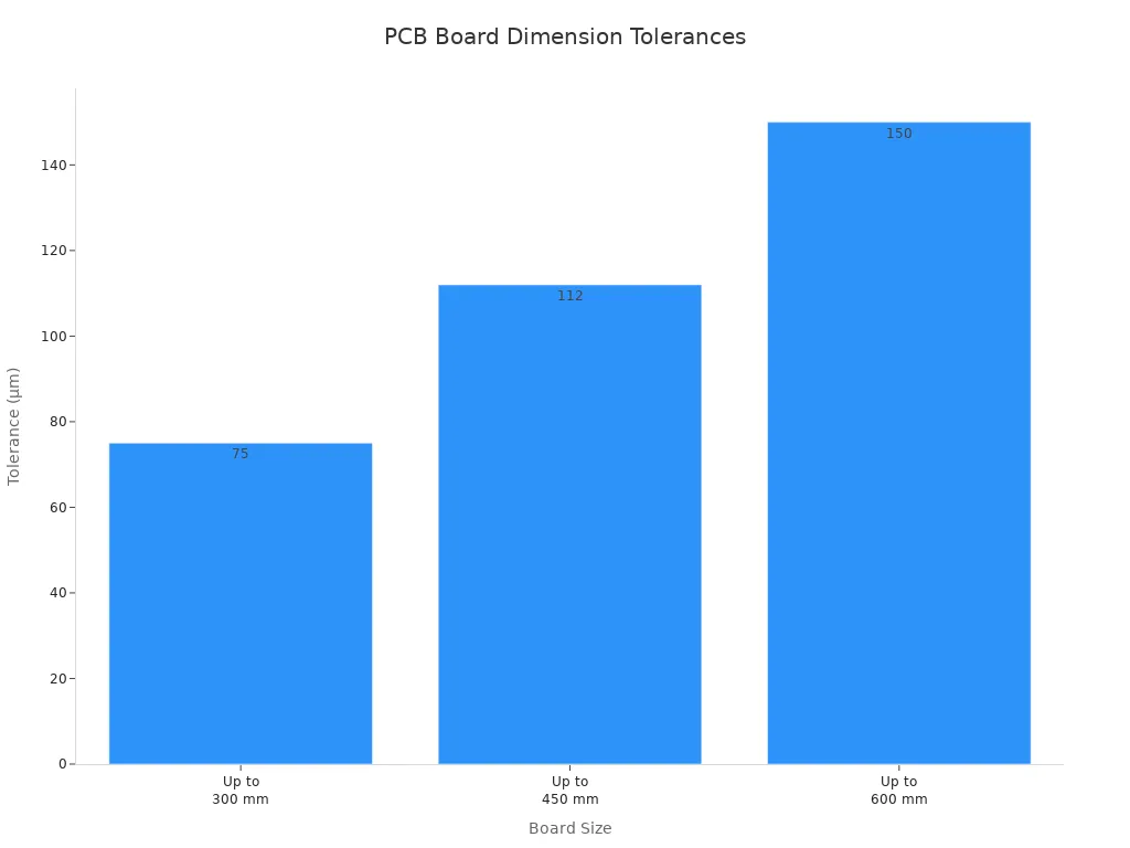
You need to check these numbers when you review your design. Following IPC rules helps you avoid mistakes and keeps your pcb ready for fast jobs.
Best Practices for Automotive PCB Design
You can stop layer stack-up and alignment mistakes by using smart steps:
Work with your manufacturer early. Talk to them when you start your design. This helps you know what they can do and avoid problems.
Use dfm rules. Make sure your design fits what the factory can make. Keep drill sizes big enough and do not use very tight spaces.
Test and check your pcb a lot. Use AOI and electrical tests to find problems early.
Tip: Always check your design before you build your pcb. Early tests help you find mistakes and make your pcb better.
You should also keep copper even, pick the right via type, and make strong power and ground planes. Good heat control stops parts from getting too hot. When you use these steps, you keep signals clear, lower emi, and avoid mistakes in fast pcb designs. Careful planning and checking help you make a strong automotive pcb.
Table of Common Layer Stack-Up and Alignment Errors
Error Type | Description | Consequences |
|---|---|---|
Unbalanced stack-up | Copper is not even, layers are not the same thickness, or signals are all on one side | Board can bend, layers can peel, and inside layers may not line up |
Incorrect via structure selection | Picking the wrong via type for your design | Signals may not work right and the board can have problems |
Inadequate power and ground plane design | Bad power or ground planes can cause voltage drops and noise | The pcb may not work well or last long |
Poor thermal management design | Not enough ways to move heat away | Parts can get too hot and stop working |
Insufficient Thermal Management in PCB
Common Thermal Design Mistakes
Good thermal management is very important in automotive pcb design. If you do not do this, parts can get too hot and break. Heat-sensitive parts like voltage regulators, MOSFETs, microcontrollers, and power ICs can stop working. Many mistakes happen when people forget thermal vias, copper pours, or heatsink areas. If you put hot parts near sensors, signals can get messed up. These mistakes can make your pcb fail and cost a lot to fix.
Forgetting thermal vias or copper pours
No heatsink areas for high-power parts
Putting hot parts close to sensors
Not thinking about heat paths in layout
Not checking heat needs during design review
Tip: Always look for heat problems in your pcb during dfm checks and tests.
IPC Guidelines for Thermal
IPC standards help keep your pcb safe and working well. You need to follow these rules for good quality and performance. IPC says to use copper planes and signal vias to move heat away from parts. Put signal vias near surface pins to help heat flow out. Add heat sinks for high-power parts. Use metal thermal pads and solid-filled vias to move heat. For tough jobs, use metal core boards. High Tg boards can handle more heat. IPC also gives rules for hole position, drill size, and hole wall space. Clean your pcb before putting on solder mask and check for problems after soldering. Follow IPC-6012DA for solder mask rules.
Note: Good thermal management stops solder joints from getting tired and keeps your pcb inside IPC defect limits.
Effective Thermal Solutions
You can use different materials and ways to fix heat problems in automotive pcb design. The table below shows choices for high-speed pcb design mistakes and how to use them:
Material Type | Temperature Resistance | Application Use Case |
|---|---|---|
FR-4 with High Tg | Up to 170°C | Less demanding automotive applications |
Polyimide | Up to 260°C | Engine control units and powertrain systems |
Ceramic-Based Materials | Superior heat resistance | High-power applications |
Metal-Core PCBs (MCPCBs) | Excellent heat dissipation | LED lighting and power electronics in vehicles |
Pick materials that match what you need and where you put them. Use thermal vias, copper planes, and good dielectrics to stop overheating. These ideas help you avoid mistakes and keep your pcb strong. Good planning and checking make your pcb better and more reliable.
Tip: Always plan for heat paths and test your pcb to meet IPC standards and stop emi.
You can save money by knowing about common mistakes in automotive pcb design. If you check your design rules and get help from experts, your pcb will be stronger and safer. You can find and stop mistakes before they turn into big problems. Planning ahead helps you follow IPC standards and keeps your work good. Always pay attention and fix mistakes early to get the best results.
FAQ
What is the most common IPC standard for automotive PCBs?
You will use IPC-6012 for most automotive PCBs. This standard covers the quality and reliability rules for rigid printed boards. Always check your project needs before you start.
How can you check for PCB design errors before manufacturing?
You can use Design Rule Checks (DRC) in your PCB software. These tools find mistakes early. You should also review your design with your team and run DFM checks.
Why do you need to follow IPC standards in automotive PCB design?
You need to follow IPC standards to keep your PCB safe and reliable. These rules help you avoid costly failures. They also make sure your board meets industry requirements.
What happens if you ignore trace width and spacing rules?
You may see overheating, signal loss, or even short circuits. Your PCB can fail IPC tests. Always set the right trace width and spacing for your design.
Can you fix PCB design errors after manufacturing?
You can fix some small errors, but many mistakes need a new board. Early checks and reviews save you time and money.
See Also
Key Challenges And Solutions In PCB Design For SMT
Seven Essential Quality Control Steps For Heavy Copper PCBs
Important Precautions To Consider When Designing PCB Boards
