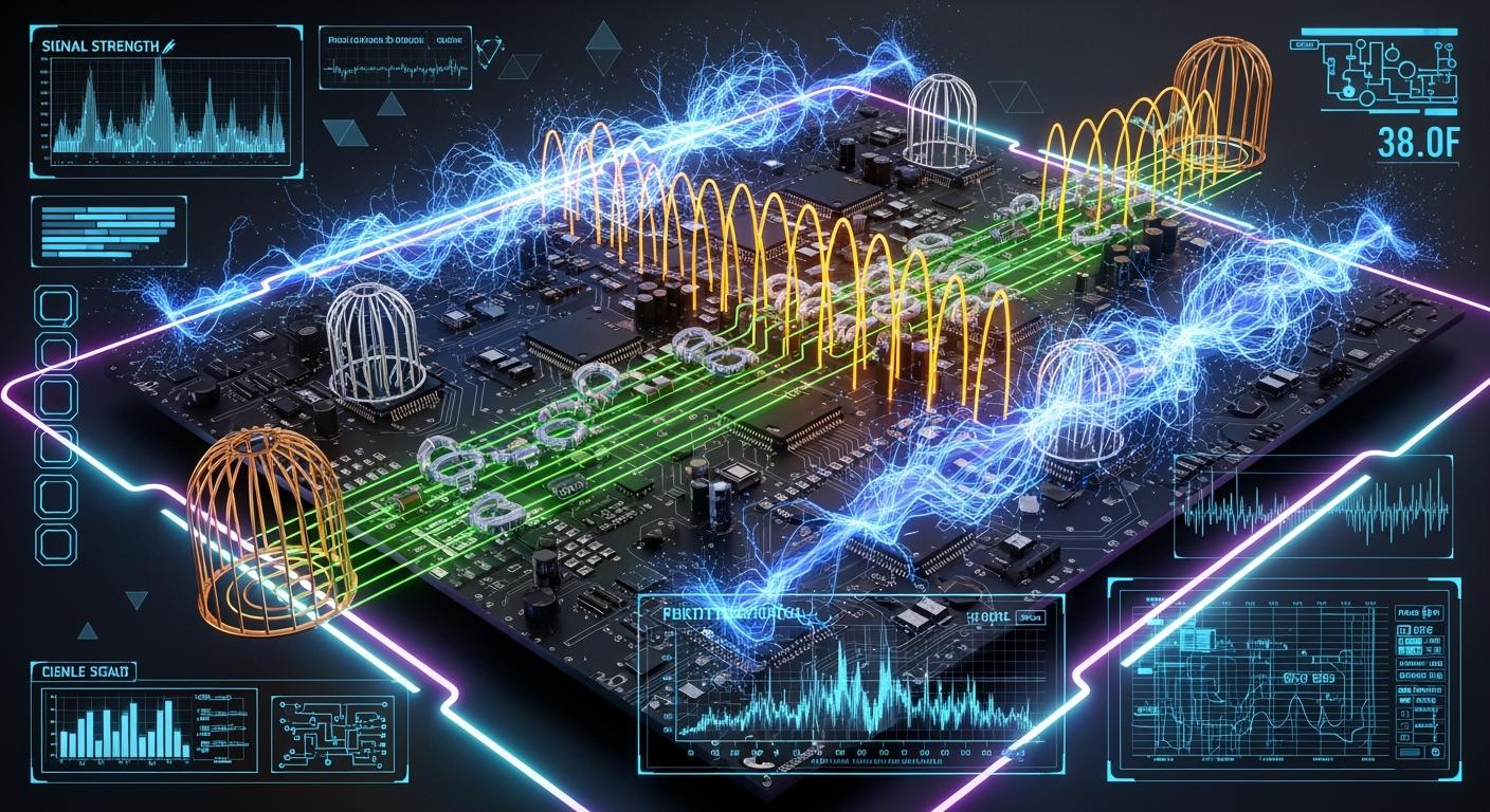
How to Suppress EMI in High-Speed PCB Designs
You can stop emi in high-speed pcb designs by using strategies that work in real life. You should use solid ground planes to keep voltage steady and cut down noise. Shielding, like grounded enclosures and conductive gaskets, helps block signals you do not want. Signal filtering with capacitors and ferrite beads gets rid of high-frequency emi. The table below lists the best ways to control emi in high-speed pcb design:
Strategy Type | Description |
|---|---|
Shielding Techniques | Grounded shields, enclosures, and conductive gaskets block emi and make attenuation better. |
Grounding Strategies | Solid ground planes lower inductance and keep your pcb steady. |
Signal Filtering | Capacitors, inductors, and ferrite beads soak up and block unwanted emi. |
You will get better results if you focus on layout, parts, and materials from the start.
Key Takeaways
Use solid ground planes to keep voltage steady and lower noise in high-speed PCB designs.
Use shielding methods, like grounded enclosures, to stop unwanted signals well.
Use signal filtering with capacitors and ferrite beads to remove high-frequency EMI.
Keep traces short and spaced right to cut down EMI and make signals better.
Do EMI testing and simulations early to find and fix problems in the design.
EMI Basics in High-Speed PCB Design
Common EMI Sources
When you design high-speed pcb, you deal with many emi sources. These can make your circuits and devices not work right. Here are some of the most common emi sources:
High-speed signals move through traces faster than 50 MHz. These traces can act like antennas and send out emi.
Switching circuits, like PWM circuits or DC-DC converters, make high-frequency noise because they switch on and off fast.
Ground loops happen when grounding is not the same everywhere. These loops can send out magnetic fields and make noise in other circuits.
Cables and connectors, especially long ones, can act like antennas. They can send out or pick up emi.
Bad pcb layout, like big loop areas or traces too close together, can make emi problems worse.
Tip: You can lower emi by making traces short and using solid ground planes in your high-speed pcb.
Why EMI Matters in High-Speed Circuits
You must control emi in high-speed pcb design because it can cause many problems. Electromagnetic interference can make noise and crosstalk, so your circuits have trouble reading signals. Lower voltage swings and smaller noise margins make signals even harder to read. When you use faster data rates or longer traces, emi gets worse and can stop your signals from going far.
EMI can make signal integrity problems in your pcb.
It can cause reflections, crosstalk, and ground bounce.
These problems change signals and make the signal-to-noise ratio lower.
You might see more mistakes when sending data.
You can make emi better by using low-inductance parts and solid ground planes. Good emi practices help you reach electromagnetic compatibility and meet emc rules. When you design for electromagnetic compatibility, your high-speed pcb works well with other devices and does not make interference.
Note: Controlling emi in your high-speed pcb design helps you avoid expensive mistakes and makes sure your board works with other systems.
PCB Stack-Up and Reference Planes for EMI
Solid Reference Planes
Solid reference planes are important in high-speed pcb. These planes give signals a clear path to return. Using a solid ground plane keeps impedance low and emi small. The ground plane stops return currents from spreading out. This helps stop noise. Signal integrity stays strong because the ground plane keeps impedance steady.
Solid ground planes make it easy for return currents to flow.
You keep emi low and your pcb works well.
Continuous ground planes help you avoid timing mistakes and extra noise.
Design checks and simulations show you the best layout.
Tip: Put your ground plane right under the signal layer. This keeps the return path short and lowers emi.
Power-Ground Plane Spacing
You need to watch the space between power and ground planes. Thin spacing helps your pcb work better. When power planes are close to ground planes, they act like a decoupling capacitor. This setup keeps voltage steady and cuts noise. It also helps with emc by keeping the supply voltage stable.
Put power planes next to ground planes with thin spacing (less than 0.254 mm).
This setup lowers emi and keeps your pcb working well.
Tight spacing stops voltage swings and ground bounce.
Multi-layer pcbs use this to block noise and interference.
Note: Do not put splits or gaps in your ground plane. Gaps break the return path and make emi worse.
Stack-Up for Signal Integrity
Plan your stack-up to keep signals clear in high-speed pcb. A good stack-up keeps impedance the same and stops reflections. Put signal layers next to reference planes. This keeps coupling tight and lowers crosstalk. You also need to manage layer spacing and routing to stop noise.
Stack-Up Tip | Benefit |
|---|---|
Signal-Ground-Power-Signal | Shields signals and lowers emi |
Ground plane under signal | Keeps return path short and stable |
Thin dielectric spacing | Acts as decoupling capacitor |
Avoid isolated signal layers | Minimizes emi and crosstalk |
A good stack-up lowers noise and controls impedance.
You keep signals strong by using ground planes as buffers and watching layer spacing.
Watch for changes in materials and how things are made. These can change impedance and hurt signal quality.
Using the right stack-up and reference planes keeps your pcb reliable.
Tip: Use design simulations to check your stack-up. Simulations help you find problems before you build your pcb.
You can lower emi in high-speed pcb by using solid reference planes, tight power-ground spacing, and smart stack-up plans. These steps keep your pcb working well, protect signals, and help you meet emc rules.
Grounding and Routing in High-Speed PCB
Multi-Point Grounding
You need to use the right grounding method to keep emi low in high-speed pcb design. Multi-point grounding works best for circuits that run above 1 MHz. This method connects the ground at many points across your pcb. You give high-frequency signals a short path to return, which lowers impedance and stops emi from spreading.
Multi-point grounding reduces the risk of ground loops.
You keep signal integrity strong by making sure the ground stays at the same voltage everywhere.
Long return paths can create ground loops that act like antennas and send out interference.
Multi-point grounding helps you avoid these problems.
You can see the main grounding techniques in the table below:
Grounding Technique | Description |
|---|---|
Signal ground vs. safety ground | Keeps signal and safety systems separate for better control. |
Low impedance path | Gives high-speed signals a fast way back to ground. |
Minimizing ground impedance | Makes emi lower by improving the ground connection. |
Ground strategies | Includes single point, multi-point, and hybrid methods. |
Ground loops | Shows what happens when grounding is not done right. |
Tip: Use multi-point grounding for high-speed pcb design to keep emi under control and protect signal integrity.
Ground Loops and Stitching Vias
You must watch out for ground loops in your pcb. These loops can cause emi and noise. They happen when you have long or broken return paths. Ground loops can act like antennas and send out unwanted signals.
Stitching vias help you fix this problem. You place these small holes in your pcb to connect ground planes on different layers. Stitching vias give high-speed signals a direct return path. This keeps the ground plane solid and stops noise from spreading.
Stitching vias keep the ground plane strong across all layers.
They lower the chance of ground loops by giving a steady ground reference.
You improve signal integrity and reduce emi by using stitching vias near high-speed traces.
Here is how stitching vias help your design:
They give high-frequency currents a low impedance path, which keeps emi inside the pcb.
They help you control impedance and keep signals clean.
They make sure return currents do not wander, which lowers crosstalk and reflections.
Note: Place stitching vias close to signal traces, especially when signals cross from one reference plane to another. This keeps the return path short and protects signal integrity.
Routing: 3W Rule, Differential Pairs, Trace Length
You need to route your traces with care to keep emi low and signal integrity high. The 3W rule helps you space traces so they do not talk to each other. You keep the edge-to-edge distance between parallel traces at least three times the trace width. This stops crosstalk and lowers emi.
Technique | Description |
|---|---|
3W Rule | Keeps parallel traces apart by three times their width to reduce crosstalk and emi. |
Differential pairs are another key tool. You use two traces that carry equal and opposite signals. This setup cancels out noise and makes your design less sensitive to interference. You must keep the spacing between these traces the same along their whole length. This keeps the signals balanced and lowers emi.
Differential pairs help you block out noise and keep signals clean.
You must route these pairs together and avoid sharp turns.
Smooth changes in direction keep emi low and protect signal integrity.
You also need to keep trace lengths short and avoid too many bends. Long traces and sharp corners can act like antennas and send out emi. Smooth, short traces keep your high-speed pcb working well and help you meet emc rules.
Tip: Use the 3W rule and route differential pairs with even spacing. Keep traces short and smooth to lower emi and keep your pcb reliable.
Filtering, Shielding, and Isolation Techniques
Ferrite Beads and Capacitors
Ferrite beads and capacitors help block unwanted emi in high-speed pcb circuits. Ferrite beads are good for power supply lines. They make high-frequency signals weaker and turn them into heat. This stops emi from moving through your board. If you put a ferrite bead in series with a power rail, you make a low-pass filter. This filter blocks high-frequency noise but lets your main signal go through.
Capacitors also help fight emi. You should put bypass and decoupling capacitors close to the power pins of your ICs. These capacitors soak up high-frequency noise and keep voltage steady. You can use different values to target different frequencies. Pi-filters use capacitors and ferrite beads together. They block emi near connectors and cables. You can also use emi filters to stop interference before it spreads.
Ferrite beads add impedance that depends on frequency.
Capacitors and ferrite beads together make strong emi filters.
Put these parts near noise sources for best emi performance.
Tip: Pick capacitor values that match the clock harmonics in your high-speed pcb design.
EMI Shielding and PCB Fencing
Shielding and fencing keep emi inside your pcb and protect signals. You can use a continuous ground plane to give return currents a low-impedance path. This lowers emi and keeps your reference voltage steady. Shielding cans and enclosures cover high-speed parts and stop interference from escaping.
Via fences use rows of vias around signal traces or board edges. These vias connect ground layers and block emi from radiating out. You should pick via sizes that fit your stack-up and keep the distance between vias small. Put high-speed parts near the center of your board. This lowers edge emissions and keeps signal integrity strong. Controlled impedance traces also help by stopping reflections and keeping signals clean.
Use a continuous ground plane for better emi performance.
Put shielding cans over sensitive or noisy parts.
Add via fences to block emi at board edges.
Note: Good shielding and fencing help you meet emc rules and keep your high-speed pcb reliable.
Separating Noisy and Sensitive Circuits
You can lower emi by keeping noisy and sensitive circuits apart. Put analog and digital parts in different areas. This stops interference from jumping between them. Use image planes under signal traces. These planes give signals a clear return path and cut down on emi.
A good layout controls crosstalk and keeps impedance steady. You can change the distance between traces and ground planes to manage signal integrity. The table below shows how isolation helps your design:
Function | Description |
|---|---|
Reducing reflow noise and EMI | Image planes lower impedance and shrink emi-causing loops. |
Controlling crosstalk | Changing trace distance controls unwanted signal coupling. |
Controlling impedance | Image planes keep impedance steady and stop reflections. |
Tip: Always keep noisy and sensitive circuits apart to protect signal integrity and lower emi.
Validation and Common EMI Mistakes
EMI Testing and Simulation
You need to check your high-speed pcb for emi before you finish. Testing helps you find problems early. You can use lab tests and computer simulations. Lab tests show if your board meets emc rules. Simulations let you see how emi moves in your design.
Here are some ways to check your design: - Make your pcb layout better by keeping traces short and using ground planes. - Add filters like ferrite beads and capacitors to block high-frequency noise. - Keep noisy parts away from sensitive circuits. - Use metal shields to cover noisy parts. - Make sure you have good grounding for return currents. - Design filters with capacitors and inductors to block unwanted signals.
You can also use industry tests to check your board. The table below shows some important tests:
Type of test | Description |
|---|---|
Radiated emissions | Measures electromagnetic radiation from your device. |
Conducted emissions | Checks emi that travels through cables. |
Electrostatic discharge (ESD) | Tests how well your device handles static electricity. |
Surge immunity | Checks if your device can survive power surges. |
Tip: Run emi simulations before you build your board. This saves time and money.
Material Selection for Low EMI
You should pick materials that help lower emi in high-speed pcb design. The right materials keep your signals strong and cut down noise. Look for materials with a low dissipation factor. This keeps signal loss small and helps your board work better. Smooth copper and good surface finishes also help. They lower conductor losses and keep data rates high.
Pick materials with low dielectric loss.
Use smooth copper to keep signal quality high.
Choose surface finishes that do not add extra loss.
Note: Good material choices help you meet emc standards and keep your pcb working well.
Mistakes to Avoid
You can stop many emi problems by watching for common mistakes: - Do not break your ground plane. This makes signals take long paths and increases emi. - Keep high-speed signals away from the edges of your pcb. - Always ground your shielding covers. If not, they can make emi worse. - Use enough decoupling capacitors to stop power noise. - Route traces short and direct. Long traces can act like antennas. - Limit how often you change signal layers with vias. - Add enough stitching vias to keep return paths short. - Terminate all high-speed lines to stop reflections.
Remember: Careful design choices help you avoid emi issues and keep your high-speed pcb working well.
You can lower EMI in high-speed PCB designs by using filters and checking insertion loss. The table below lists important steps:
Key Practice | Description |
|---|---|
EMI suppression filters | Filters take out noise from signals by using frequency differences. |
Insertion loss measurement | Measures how well filters stop unwanted noise. |
You should start working on EMI control early in your design. Cloud-native platforms let your team work together and find problems quickly. Automated rule checks and AI routing tips help keep your design safe from EMI.
Teams can look at and change designs at the same time.
Rule checks run all the time and show problems early.
AI tools help you spot signal problems before they get worse.
FAQ
What is the most effective way to reduce EMI in high-speed PCB designs?
You get the best results by using solid ground planes and keeping traces short. Place decoupling capacitors close to ICs. Use shielding and proper stack-up. These steps help you control EMI and keep your board reliable.
How do ferrite beads help with EMI suppression?
Ferrite beads block high-frequency noise. You place them on power lines or near connectors. They act like filters and turn unwanted signals into heat. This keeps your signals clean and lowers EMI.
Should you always use differential pairs for high-speed signals?
You should use differential pairs for high-speed signals when possible. They help cancel out noise and reduce EMI. Keep the spacing between the two traces even. This keeps your signals balanced and strong.
Can PCB material choice affect EMI?
Yes, PCB material affects EMI. Materials with low dielectric loss and smooth copper keep signals strong. They help reduce noise and improve signal quality. Choose materials that match your design needs for the best EMI performance.
What is the 3W rule in PCB routing?
The 3W rule means you keep parallel traces at least three times their width apart. This reduces crosstalk and lowers EMI. Use this rule when routing high-speed signals to keep your board working well.
See Also
Important Considerations When Designing PCB Circuit Boards
Top Materials Recommended for High-Speed PCB Development
The Role of Impedance Control in Enhancing Signal Integrity
Key Guidelines for Creating Heavy Copper PCBs for High Currents