How to Avoid Costly PCB Via Design Errors in 2026

You can stop expensive PCB Via Design mistakes in 2026 by following some important steps. Begin with picking the right via and handle aspect ratios to make things work better. Watch out for thermal reliefs and always talk with your manufacturer. Many engineers pick vias that are too tiny, put vias inside BGA pads without filling them right, or leave vias open, which causes big problems. If you take time to use best practices, you can save money and keep your PCB working well.
Key Takeaways
Pick the correct via type for your PCB. This helps signals stay strong and heat move well. - Watch aspect ratios closely. This stops weak plating and keeps connections safe. - Always add thermal reliefs on power and ground planes. This makes solder joints better. - Work with your manufacturer early. This helps find design problems and saves money. - Use checklists to follow design rules. This stops expensive mistakes.
Common PCB Via Design Mistakes
When you make a PCB, you can make mistakes. These mistakes can make your board not work well. They can also make it cost more money. If you know about these mistakes, you can stop them. This helps you save money and make your pcb via design better. Let’s see what mistakes happen a lot and how they hurt your board.
Skipping Thermal Reliefs on Power/Ground Planes
If you do not use thermal reliefs, you can have big problems. Power and ground planes need thermal reliefs. Big copper areas take heat away from solder joints. This makes soldering hard. You might see:
Heat does not spread evenly when soldering
Solder joints do not stick well
Fast heat loss causes stress
Solder joints crack or parts break later
Tip: Always put thermal reliefs on vias in power and ground planes. This keeps heat even and makes your board last longer.
Improper Via-in-Pad Filling
If you use via-in-pad, you must fill the via right. If you do not, you can have trouble like:
Water gets in and causes rust or shorts
Connections break and circuits do not work
Air or flux gets trapped and hurts solder joints
Empty spots make the connection weak
Via-in-pad is hard to do. It needs filling, flattening, and capping. These steps can make the board cost 15-30% more. If you skip them, you may pay more to fix problems.
Exceeding Via Aspect Ratio Limits
Each via has a limit for how deep it can go. This is called the aspect ratio. If you go past this limit, the plating gets weak. Here are the aspect ratio limits for 2026:
Via Size | Maximum Aspect Ratio | Maximum Board Thickness |
|---|---|---|
20/10mil | 1:6.4 | 2.5mm |
22/12mil | 1:10 | 3mm |
18/8mil | 1:8 | 1.6mm |
16/6mil | 1:6.7 | 1mm |
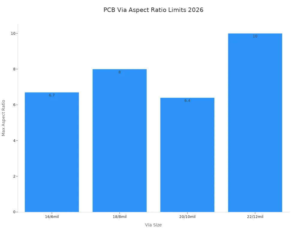
If you do not follow these rules, you can get thin plating. You might also see barrel cracks and open circuits.
Inadequate Via Plating
Bad plating is a common mistake in via design. You might see:
Barrel cracks from heat and cold
Thin copper walls or empty spots from bad plating
Layers come apart from bad materials
The board bends from stress during making
Plating problems from too big aspect ratios or different via sizes
These problems make your board less reliable. They can also stop signals from working.
Poor Via Type Selection
Picking the wrong via type can cause problems. It can hurt signals and heat control. Here is how different via types compare:
Via Type | Impact on Signal Integrity | Impact on Thermal Performance |
|---|---|---|
Through-hole | Makes long stubs that hurt signal integrity | Gives strong mechanical strength |
Blind | Makes stubs shorter and lowers inductance | Keeps the surface smooth |
Buried | Shorter via barrel helps signal integrity | Helps heat control in tight spaces |
If you pick the wrong via, signals may not work well. Your board can also get too hot in some places.
Ignoring DFM Guidelines
If you do not follow design for manufacturability rules, you can make costly mistakes. You should:
Use fewer vias in fast signal paths
Make sure via size and pad size fit the rules
Do not put important signals over split planes
Note: Always talk to your fabricator early. Use calculators for impedance and check if materials are ready before you finish your design.
Overlooking Signal Integrity
If you forget about signal integrity, you can get problems. These problems include impedance mismatches and reflections. This can cause:
Eye diagrams to close
More bit errors
Timing problems
You may not see these problems until you test the board. Fixing them later can cost a lot of money.
Practical Examples of Common Mistakes
Here are some real ways these mistakes can hurt your board:
Issue Type | Impact on Reliability | Cost Implications |
|---|---|---|
Solder Wicking | Not enough solder makes weak joints | More money spent fixing bad joints |
Voiding | Connections are not reliable | You may pay more for warranty claims |
Cold Solder Joints | High-power parts may not last long | More failures and higher costs |
Thermal Issues | Bad heat flow can break parts | You may need to spend more on cooling |
If you follow good design rules and know about these mistakes, you can make your board work better and save money.
Reliable PCB Via Design Steps
Choose the Right Via Type
You have to pick the best via for your pcb. Each via type does something different. Through-hole vias make the board strong. Blind and buried vias help signals and heat move better. Microvias are good for boards with lots of parts close together. If you use via-in-pad, fill the via so solder does not leak. Non-conductive fill keeps solder joints strong. Conductive fill helps with heat and makes the board stronger. Always choose the via type that fits your board.
Tip: Use microvias for fine-pitch BGAs and HDI boards. Blind and buried vias help stop signal loss in fast circuits.
Manage Aspect Ratio
You need to control the aspect ratio for each via. This means how deep the via is compared to its width. Keeping the ratio low makes building the board easier. It also makes the board last longer. High aspect ratios can cause problems with plating and signals. Try to keep the ratio under 10 to 1 for through-hole vias. Use microvias or buried vias for boards with lots of parts.
Best ways to manage aspect ratio:
Pick ratios that are easy to make so you avoid mistakes.
Choose ratios that protect signals and stop extra effects.
Use microvias or buried vias when space is tight.
Select Proper Materials
You need to pick the right materials for your pcb. Good materials make the board work better and last longer. Some materials are best for high-frequency boards. Others cost less and work for most boards. Look at the table below to see which materials fit your board.
Material Type | Characteristics | Application Use Case |
|---|---|---|
FR-4 | Cost-effective, suitable for many applications | General PCB designs |
Rogers RO4000 series | Low-Dk/Df, reduces signal loss | High-frequency designs |
Megtron | High-performance laminate | Advanced signal integrity applications |
Isola materials | Low-loss materials for high-speed applications | High-frequency and HDI boards |
Thinner dielectrics | Improves impedance control and via reliability | HDI boards |
Note: Thinner dielectrics help control impedance and make vias stronger in HDI boards.
Ensure Quality Plating
You must make sure the copper inside each via is thick and even. Good plating keeps connections strong and stops cracks. Bad plating can cause barrel cracks and open circuits. Always follow IPC rules for filling and plating vias. Use pulse plating for vias with high aspect ratios. Test your board with heat and shaking to check if it is strong.
Quality Control Measure | Description |
|---|---|
Adhere to IPC Standards | Follow IPC standards for via filling materials and processes to ensure reliability. |
Control Manufacturing Parameters | Maintain tight tolerances during via drilling and filling as per IPC-6012E criteria. |
Perform Reliability Testing | Conduct thermal cycling and vibration testing to validate design under real-world conditions. |
Tips for good plating:
Make sure each via has at least 25 µm (1 mil) copper.
Use pulse plating for even copper in high aspect ratio vias.
Test filled microvias for heat, shaking, and wetness.
Collaborate with Manufacturer
You need to work with your pcb maker. Share your design early and ask for their ideas. Use online tools to update your design fast. This helps you stop expensive changes later. Good talking makes sure your design follows the rules. Teams working together can find ways to save money and make the board better.
Why working together helps:
Sharing data fast makes updates easy.
Good talking makes sure the board can be built.
Teams can find ways to save money.
Tip: Check the DFM report from your manufacturer before you send Gerber files.
Use Design Rule Checklists
You should always use a checklist for pcb via design. Checklists help you follow the rules and stop mistakes. Look over your stackup, trace width, spacing, and where you put vias. Make sure you follow IPC rules and keep parts away from the board edge. Write down your layer stackup and notes for making the board.
PCB via design checklist for 2026:
Minimum trace width: 6 mils for 1 oz copper
Minimum spacing: 8 mils
Minimum annular ring: 5 mils
Do not put vias under parts unless needed
Part clearance: 50 mils for high-power, 20 mils for normal
Solder mask clearance: 4 mils around pads
Standard drill sizes: 10 mils or bigger
Board edge clearance: 10 mils
Panelization set for best yield
Stack-up locked and impedance checked
Differential pairs matched in length
No fast signals crossing plane splits
Decoupling caps within 1–2 mm of power pins
Copper balanced within ±10% on all layers
Three fiducials, two tooling holes, solder mask checked
Silkscreen does not touch pads
DFM report checked before sending Gerber files
Callout: Using a checklist helps you find mistakes early and keeps your pcb strong.
If you follow these steps, your pcb via design will be strong and save money. If you pick the right via, control aspect ratio, choose good materials, make sure plating is good, work with your manufacturer, and use checklists, your board will work better. These steps help you stop mistakes and make your board last longer.
Practical PCB Tips and Checklists
Pre-Layout Planning
You start by planning where each part will go. You keep enough space between traces, pads, and masks. Annular rings around vias help keep plating strong. Place important parts like Buck Regulators first. Do not put random parts close to big chips. Leave space for routing around BGAs and big packages. Talk with your manufacturer about layers and panelization. Check solder mask clearance and the smallest trace width.
Tip: Planning early helps stop signal problems and lowers noise.
Schematic and Stackup Review
You look over your schematic and stackup before layout. Make sure every signal path is clear. Check if the stackup fits your design goals. Count the layers to see if you have enough for routing. Make sure the stackup lets you put vias in the right spots. Look for missing connections or mistakes in the schematic.
Review Step | What You Check |
|---|---|
Signal Path | No broken or missing connections |
Layer Count | Enough layers for routing |
Stackup | Supports via placement and impedance |
Schematic | Matches layout requirements |
Layout and Routing
Use fewer but wider vias to make routing better. Keep trace widths and spacing correct. Use differential pair routing to stop skew errors. Plan escape routes for BGAs before you start routing. Run design rule checks often to catch mistakes early.
Callout: Running DRC checks many times helps you find problems before they cost more.
DFM Review
Follow steps to make your pcb easy to build.
Keep to minimum keep-out zones and spacing rules.
Use filled and plated-over vias for via-in-pad.
Check IPC standards for spacing and copper weight.
Work with your manufacturer early to stop mistakes.
Design within what your fabricator can do. Do not use very thin traces or odd materials. Check for crowded parts and missing info in fab files.
Note: Working with your manufacturer early helps you avoid delays and extra costs.
Advanced Vias and Trends for 2026
New Materials and Via Technologies
New materials and technologies are changing how vias are made. Engineers use ceramic because it handles heat well in strong electronics. Polyimide is used for flexible pcbs because it bends and lasts a long time. Metal core boards help move heat away in LED lights and other powerful devices. Micro-vias and via-in-pad let you put more parts in a small space. Nano vias are even smaller than microvias, so boards can be tiny and hold more. Biodegradable boards are getting popular because they help cut down on waste.
Material/Technology | Description | Advantages |
|---|---|---|
Ceramic | Handles heat very well | Stays stable when hot |
Polyimide | Bends and takes high heat | Strong and flexible |
Metal Core | Moves heat away fast | Better at cooling |
Micro-Vias | Tiny holes link layers | Makes boards small and fast |
Vias inside part pads | Saves space and connects well |
Tip: Using new materials and via types helps your boards last longer and work better.
IPC Standards Updates
You need to follow new IPC standards to make sure vias work well. IPC-6012E gives rules for how plated holes should look, which is important for microvias. IPC-4761 tells you how to protect and fill vias, making boards stronger. IPC-6012 checks if finished boards meet the right standards. These rules help you design better and stop expensive mistakes.
IPC-6012E gives rules for plated holes.
IPC-4761 helps protect and fill vias.
IPC-6012 checks if boards meet standards.
Note: Following IPC rules keeps your vias safe and strong.
HDI and Microvias
HDI boards use microvias instead of big through-holes. This gives you more room to route and lets you use tiny parts. You need to keep the aspect ratio right for good plating and heat control. Laser drilling works better than regular drilling for making deep vias. You must pick materials that work well together and handle heat changes. If you do not, microvias can break. Even small changes in material can mess up signals. Bad microvias can cause open circuits and make boards fail sooner.
Microvias give you more space and let you use small parts.
Laser drilling makes deep vias better.
Picking the right materials and handling heat is important.
Callout: Always count how many laminations your HDI board has, because it changes the cost and how hard it is to make.
Automation in Via Design
Automation makes designing vias faster and more correct. AI tools help you lay out parts, save space, and keep signals clear. Automated systems find problems early and check if your design can be built. Robots and smart factories watch the process and fix mistakes right away. Automated lines help you spend less money and make boards that are always the same.
AI tools help you plan layouts.
Automation stops mistakes and keeps quality high.
Robots watch and fix things as they happen.
Tip: Using automation in via design helps you find problems early and make better boards.
Preventing PCB Via Failures
Identifying Failure Risks
You need to spot risks early to stop pcb via failures. The most common risks in 2026 include cracks in the via barrel, poor copper plating, and weak solder joints. Sometimes, you see voids inside the via. These voids can break the electrical path. If you use high-speed signals, you may face signal integrity problems. Vias that do not match the board design can cause open circuits or make the board fail during heat cycles. You should check for uneven plating, wrong via size, and missing fills. These issues often lead to costly repairs.
Tip: Always review your design for signs of stress or poor plating before you send your pcb for manufacturing.
Testing and Inspection
You must test and inspect every via to keep your pcb strong. Use X-ray inspection to find hidden cracks or voids. Thermal cycling tests show if the via can handle changes in temperature. You can use cross-section analysis to check the copper thickness inside the via. Electrical tests help you find open circuits or weak connections. If you run these tests, you catch problems before the board fails in the field.
Test Type | What It Finds |
|---|---|
X-ray Inspection | Cracks, voids, missing fill |
Thermal Cycling | Barrel cracks, solder issues |
Cross-section | Copper thickness, plating |
Electrical Test | Open circuits, weak joints |
Callout: Testing and inspection help you keep your design reliable and avoid expensive fixes.
Addressing Thermal and Mechanical Stress
You can stop failures by making smart design choices. Try these methods:
Use conductive fill in vias to boost thermal conductivity and mechanical strength. This works well for power or RF boards.
Choose non-conductive fill to prevent solder wicking. You avoid poor solder joints.
Optimize copper plating with pulse plating. This gives you uniform copper and keeps the via stable.
Select the right via types. Microvias and backdrilled vias improve mechanical performance and signal integrity.
Use high-performance materials. High-Tg substrates and low-CTE laminates help your pcb resist heat and reduce expansion mismatch.
If you follow these steps, you protect your design from stress and keep your vias strong. You also lower the risk of signal integrity problems and make your pcb last longer.
Note: Good design and careful material selection help you avoid pcb via failures and keep your board reliable.
You can avoid costly mistakes in pcb via design by following clear steps. Use checklists to catch errors early. Work closely with your manufacturer to make your board reliable. Stay updated with new standards and trends. Keep learning and use tips to improve your designs.
Remember: Smart planning and teamwork help you build strong boards that last.
FAQ
What is the best way to choose a via type for my pcb?
You should look at your board’s needs. If you have tight spaces, use microvias. For strong connections, pick through-hole vias. Ask your manufacturer for advice.
How can I prevent via failures during manufacturing?
You can use quality materials and follow IPC standards. Test your board with X-ray and thermal cycling. Work with your manufacturer to check for common mistakes.
Why do aspect ratios matter in via design?
Aspect ratios show how deep a via is compared to its width. If you keep the ratio low, you get strong plating and fewer cracks. High ratios can cause weak connections.
What is the role of thermal reliefs in via design?
Thermal reliefs help heat spread evenly during soldering. If you use them, you get better solder joints and fewer failures. Always add thermal reliefs to power and ground planes.
How do I check if my via design follows DFM guidelines?
You can use a checklist. Look for correct spacing, pad size, and filled vias. Review your design with your manufacturer. This helps you avoid costly mistakes.
See Also
Effective Ways to Reduce Expenses in Custom PCB Manufacturing
Essential Considerations for Designing PCB Circuit Boards
Best Practices to Lower Back Drilling Costs in HDI PCBs