In-house Laser Production for High-Precision PCB
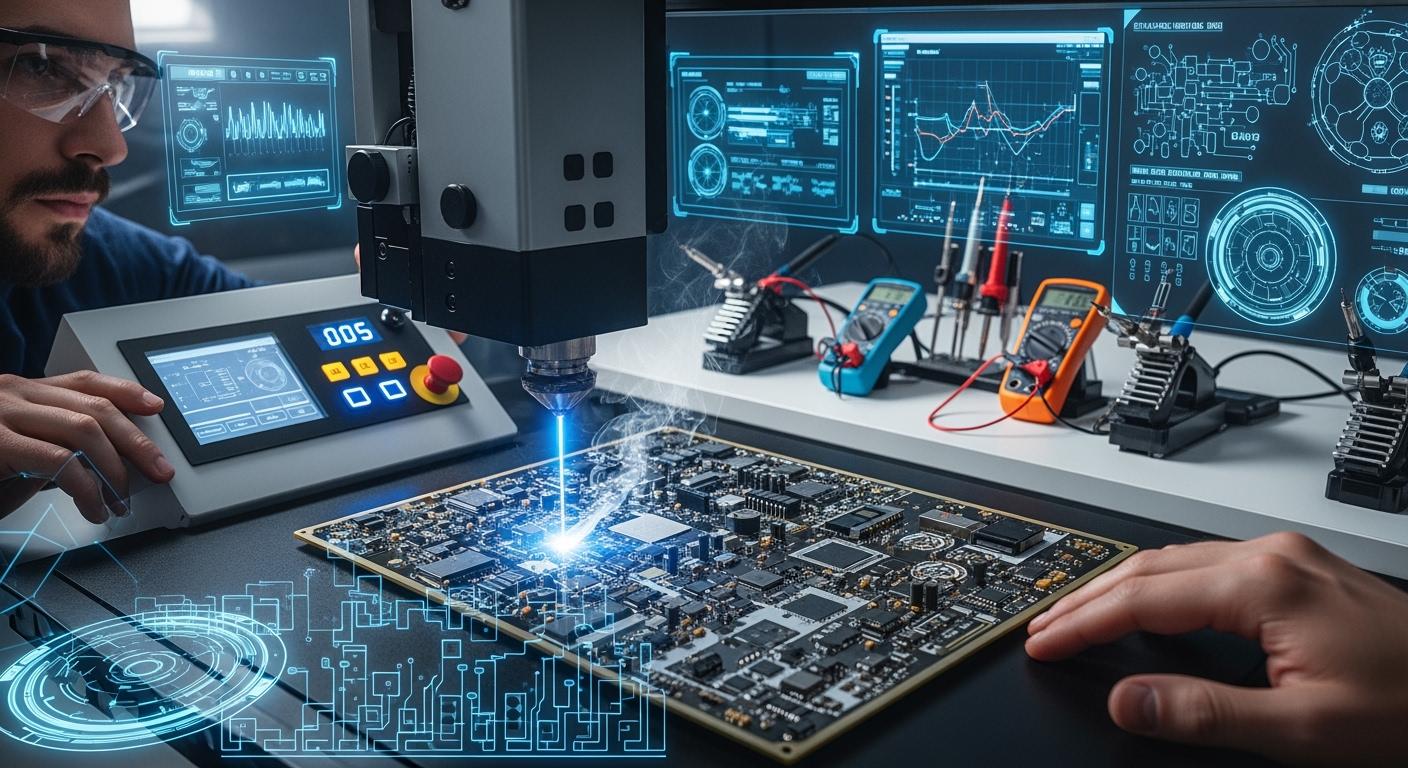
In-house laser production lets you make high-precision PCB in your own building. You use focused laser beams to shape and mark circuit boards without touching them. This way gives you more control and helps you change designs quickly.
Small laser systems fit easily in labs and help you finish R&D work faster.
Here is how laser-based processes make PCB manufacturing better:
Advantage | Explanation |
|---|---|
Mechanical Precision | Laser cutting gives you very accurate features near circuits. |
Stress-Free | No shaking or rubbing means your boards stay safe and last longer. |
Low HAZ | UV laser ablation stops melting, so you avoid short circuits. |
Operational Flexibility | You can cut any shape and change production fast. |
Material Independent | Lasers work with almost any PCB material you pick. |
Laser direct imaging now lets you put patterns on boards faster and with less waste. You can meet the needs of smaller and more complex devices more easily.
Key Takeaways
Making PCBs with lasers in your own shop lets you control designs. It also helps you finish work faster.
Lasers make things more accurate and quick. They help you make small details without hurting the PCB material.
Using lasers means less waste and less harm to the environment. You do not need bad chemicals and you use less material.
People must learn how to use laser machines safely. This keeps everyone safe at work.
Laser systems need regular care and checks. This helps PCBs stay good and work well every time.
What Is In-house Laser Production for PCB?
Core Principles of Laser PCB Manufacturing
Laser technology helps you make a pcb with better accuracy. Older methods use chemicals or drills. These ways can hurt the board. Lasers do not touch the material. This keeps the board safe from cracks.
Laser drilling makes tiny holes, as small as 0.025 mm. This is needed for high-precision pcb designs.
You can drill thousands of holes every minute. This lets you finish complex pcb layouts quickly.
Laser systems do not break down like drills. You get the same results each time.
Small machines, like the LPKF ProtoLaser H4, work with many pcb materials. You can cut pads, traces, and tiny holes with good control.
Automated laser systems help you avoid mistakes. You get steady results for every high-precision pcb.
Here is a table that shows the main principles and how they help you:
Core Principle | How It Helps You Achieve High-Precision PCB |
|---|---|
Maskless Lithography | You can change designs fast without making new masks. |
Laser Direct Imaging (LDI) | You get resolutions down to 10 microns for detailed circuits. |
Multilayer Board Handling | You line up traces and vias with high accuracy. |
Scalability | You can make smaller and more complex pcb for new devices. |
Cost Efficiency | You save money by cutting waste and errors. |
Design Flexibility | You can try new layouts without limits from masks. |
Environmental Benefits | You avoid chemical waste and help green practices. |
Relevance for High-Precision PCB
High-precision pcb is needed for advanced electronics. Laser technology gives you tools to meet these needs.
Laser drilling lets you make tiny vias. These are important for high-density pcb.
You keep tight tolerances, so your circuits work well at high speeds.
The laser process does not touch the pcb layers. This lowers the risk of damage.
Every hole and trace stays the same size and shape. This keeps your signal quality high.
Small laser systems, like the LPKF ProtoLaser H4, let you make quick changes during prototyping. You can test and improve your high-precision pcb designs faster.
Tip: If you want to keep up with new technology, in-house laser production gives you the speed and accuracy you need for modern pcb projects.
Benefits of Laser-Made PCBs
Precision and Speed Advantages
Laser-made pcbs help you work with great accuracy and speed. Lasers can make very tiny details on your pcb. They can mark and cut things that are super small. This is important for small parts and tricky designs. You do not have to worry about tools breaking or making mistakes. The laser always does the job the same way.
Here is a table that shows how laser-made pcbs are different from old ways:
Advantage Type | Description |
|---|---|
Precision | Laser marking makes very fine marks. It can do this for small parts and hard designs. |
Speed | Laser marking is fast. It helps you finish work quickly and saves time and money. |
You can finish your pcb jobs much faster. The laser works quickly and skips steps like making masks or using chemicals. You can go from your idea to a finished board in less time. This speed helps you meet deadlines and keep your work on track.
Laser-made pcbs also give you good accuracy. Every trace and hole will be the right size and in the right spot. This is important for high precision work, especially for advanced electronics.
Waste Reduction and Prototyping Efficiency
Laser-made pcbs help you make less waste and work better. You do not need to use chemicals or inks. This means you do not make harmful waste. You also do not have to handle dangerous stuff, which saves time and money.
You do not need inks or solvents, so you do not have to deal with dangerous waste.
Laser etching does not use bad chemicals, so there is less pollution and waste.
No chemicals means no bad waste is made, which is better for the planet.
Laser etching is very accurate and helps you use less material.
You can change designs fast without needing new tools, so you make less waste.
You can also change your pcb designs quickly. Laser-made pcbs let you try new ideas and test them fast. You do not have to wait for new tools or masks. You can design, make, and test a pcb in just a few hours. This helps you find and fix problems early. Your final product will work better.
Quick turn pcbs are made and put together fast, so you can meet tight deadlines.
They cut down the time it takes to make a pcb from weeks to days or even hours, which is great for testing ideas quickly.
You can test and fix designs fast, so you find problems early and your final product is better.
Laser-made pcbs give you the accuracy and high precision you need for new projects. You can work faster, make less waste, and improve your designs every step.
PCB Laser Marking Machines and Setup
Essential Equipment and Facility Needs
If you want to use pcb laser marking machines, you need the right tools and space. These machines help you cut, mark, and shape your pcb. Your lab must have enough power. You also need compressed air and a good exhaust system. These things help your machines work safely.
Here is a table that shows what you need for your setup:
Description | |
|---|---|
Machine vision | Helps you find board markings for accurate cutting |
Standalone or SMT line integration | Lets you use machines alone or with other pcb tools |
Laser sources | CO2 or UV lasers for different pcb cutting jobs |
Frame construction | Strong steel frame with aluminum panels for long use |
PCB conveyor | Moves boards up to 20″ x 18″ for easy cutting |
Emergency stop button and safe laser workstation | |
Automatic board handling | Slots with safety locks for safe board movement |
User interface | Monitor, keyboard, and touchscreen for easy control |
Software | LaserGraf5 software on Windows® 10 for smooth operation |
Laser safety | Safety windows and Class 1 laser system |
Laser source type | XY gantry laser for precise cutting |
Fume extraction system | Removes smoke and keeps air clean during cutting |
Dimensions | 39.38in x 63.50in x 62.50in for lab fit |
You should plan your lab space for these machines. Make sure you have room for the conveyor and fume extraction. Good planning helps you use your pcb laser marking machines for all your cutting jobs.
Staff Training and Safety
Your team needs training before using pcb laser marking machines. Training keeps everyone safe and helps you get good results. Teach your team to wear laser safety glasses, protective clothes, and masks. These items protect them from laser light and fumes.
Follow these safety steps:
Always use the right protective gear.
Keep laser beams away from people with barriers and locks.
Give full training on how to use the machines and what to do in an emergency.
Follow OSHA rules and put clear labels on all laser cutting machines.
Check your lab often to make sure you follow all safety rules.
You should use machines with safety features like interlocks, warning lights, and emergency stop buttons. Regular checks and good training help you avoid accidents. This keeps your pcb laser marking machines working well. When you focus on safety and training, your lab becomes a safer place for cutting and marking pcb.
Implementation Steps for High-Precision PCB
Planning and Installation
You need a good plan before starting high-precision pcb work with lasers. Planning helps you avoid mistakes and keeps your work on track. Here are the main steps you should follow:
Select the Right Laser Drilling Machine for PCB
Pick a machine that works with your pcb material. Think about the hole size and how many boards you want to make. The right machine helps with both testing and making lots of boards.Prepare Your Workspace for Laser Drilling
Set up your lab with good air flow and a strong table. Make sure you have enough power for the laser. A clean and safe space helps you get better results.Install and Configure Laser Drilling Software
Put the software on your computer and set it up for your needs. The software lets you control the laser and helps you make and test boards quickly.Calibrate the Laser Drilling Machine for Precision
Adjust the machine so it drills in the right spot. Calibration is important for high-precision pcb work and keeps your design correct.Test the System with a Sample PCB
Try the machine with a sample board. Check if the laser drilling works as you want. Testing helps you find problems early.Implement Laser Drilling Safety Measures
Teach your team about safety. Use goggles, masks, and follow all safety rules. Safe habits protect people and equipment.Maintain the Laser Drilling System for Longevity
Clean and check your machine often. Good care keeps your laser working well and helps you make more boards.
Tip: Good planning and setup help you move from testing to making lots of boards without delays.
Calibration and Workflow Integration
You must calibrate your laser system before making pcbs. Calibration makes sure your drilling is correct and matches your plan. Here are important steps for calibration and workflow:
Check the laser focus and adjust it for your pcb material. This step helps you avoid damage and keeps your design sharp.
Learn how heat from the laser affects your board. Too much heat can hurt your pcb. Set the right power for each material.
Clean the laser optics often. Dust or dirt can change the laser beam and make your drilling less accurate. Clean optics help you get the same results every time.
Test your workflow with a simple design. Run a small batch of boards to see if the laser drilling fits your needs. This test helps you find problems before making lots of boards.
Update your workflow to include laser drilling steps. Add checks for calibration and cleaning. This update helps you work faster and keeps your process smooth.
Note: Regular calibration and workflow checks help you keep your pcb work correct and your testing fast.
You can add laser technology to your current pcb line. Start with small batches and easy designs. Train your team to use the new system. Over time, you will see better results in both testing and making boards. Your design process will get faster, and you will waste less material.
Step | Why It Matters for PCB Fabrication and Prototyping |
|---|---|
Keeps drilling correct and design on target | |
Makes sure laser steps fit with other jobs | |
Regular Maintenance | Stops errors and helps you make more boards |
Staff Training | Helps your team use new tools safely and well |
If you follow these steps, you will make better pcbs, test faster, and get the most from your laser drilling technology.
Challenges and Solutions in Laser PCB Production
Technical Issues and Maintenance
When you use laser marking equipment for modern pcb manufacturing, you might run into some problems. These problems can make your marking less accurate or hurt your pcb quality. Sometimes, the material you use can cause trouble too. Lasers can also have issues if you do not take care of them. You can fix these problems by changing how the laser works, keeping your workspace clean, and picking the right materials. The table below shows some common problems and how to fix them:
Technical Issue | Typical Resolution |
|---|---|
Precision and via quality issues | Adjust laser parameters |
Material constraints | Clean materials and ensure good ventilation |
Scalability problems | Use professional fabrication for multilayer boards |
Long-term reliability risks | Clean with isopropyl alcohol and apply protective finishes |
It is important to keep your laser marking equipment in good shape. Here are some tips for taking care of your machines: Keep your work area clean and wipe off camera lenses and sensors often. Watch the temperature and humidity so your laser marking equipment stays safe. Teach your team to look for problems early. Use good parts when you need to fix something. Always save your software settings and data.
If you do these things, your laser marking equipment will work well. You will get strong, clear marks on every pcb.
Training and Troubleshooting
Learning to use laser marking equipment for pcb production can be tricky. The technology can be hard to understand. Some teams have a hard time finding people who know how to use it. The chart below shows the biggest training problems:
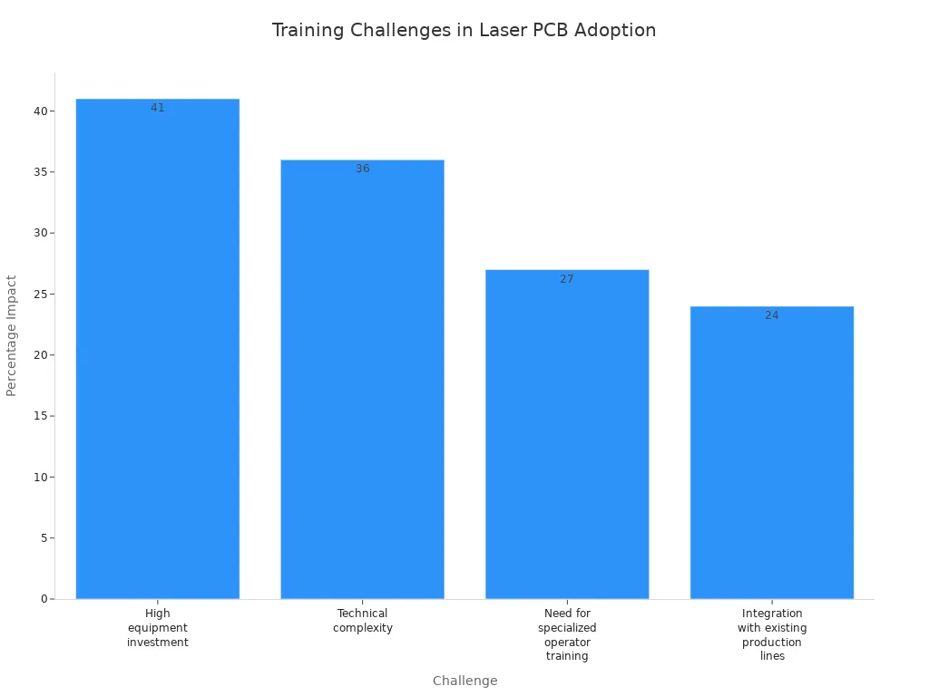
You can see that buying the equipment and learning how to use it are the hardest parts. More than 25% of workers have trouble getting used to new laser marking systems. This can cause mistakes and make the quality worse.
To fix these problems, you should make a cleaning schedule for your laser marking equipment. Check fluid levels and change cleaning liquids often. Put oil on moving parts every month. Teach your staff how to use the machines safely. Have experts check your machines to find problems early.
People who use laser marking equipment say you get better results if you pick the right materials, drill microvias one layer at a time, and check your laser marking equipment often. Cleaning after drilling and working with your team on design rules also help you get better marks and more reliable results.
Tip: If you spend time on training and follow a good troubleshooting plan, your team will get better at their jobs and your modern pcb manufacturing line will work well.
You get lots of good things when you use laser production in your own building for high-precision PCB. You make circuit cuts that are clean and do not cause stress. You finish your boards faster. You can check the quality at every step. You also save money, sometimes up to 40%.
Benefit | Description |
|---|---|
Tighter Quality Control | You watch each step to get steady results. |
Faster Lead Times | You avoid waiting and finish boards fast. |
Improved Yield | Precision helps you make more boards that work. |
Think about using this technology. It helps your PCB projects stay quick, dependable, and ready for new ideas.
FAQ
What is the main advantage of using lasers for PCB production?
Lasers help you make PCBs with more accuracy and speed. You can add tiny details and change designs quickly. Lasers do not wear out like other tools. This means you make fewer mistakes. It is easier to build advanced PCBs for new devices.
Do I need special training to use PCB laser machines?
You must get training before using these machines. Training teaches you how to use the machine safely. You learn about safety gear and how to control the machine. You also learn what to do in an emergency. Training keeps your team safe and helps you work better.
Can laser systems work with different PCB materials?
Lasers can cut many types of PCB materials. They work on FR4, ceramics, and flexible boards. You pick the right laser for your material. This lets you try more ideas for your designs.
How does laser PCB production help the environment?
Laser PCB production makes less waste. You do not need to use harmful chemicals. This means less pollution and you save materials. Your lab can be more eco-friendly.
What safety features should I look for in a laser PCB machine?
You should look for emergency stop buttons and safety windows. Interlocks are also important for safety. These features keep you safe from laser light and accidents. Your workspace stays safe and you follow the rules.
See Also
How Vacuum Two-Fluid Etching Machines Enhance PCB Precision
Exploring LT CIRCUIT's Capabilities for Complex PCB Designs
Understanding the Process of HDI PCB Laser Via Filling
In-House PCB Manufacturing: All-Inclusive vs. Partial Approaches
