10 Critical Medical PCB Design Pitfalls Every Engineer Should Know

You have a hard job when you design medical pcb. You need to follow strict rules and make sure devices always work. If you make one small mistake, it can hurt patients or slow your project. If you think about safety and rules early, you can stop expensive mistakes in medical pcb design.
Following rules means you need correct papers and clear suppliers.
Problems with rules can bring risks and make medical device design slower.
You must follow safety rules, substance limits, and keep good records for pcb to work well.
Checking your design early and learning new rules keeps your device and your good name safe.
Key Takeaways
Begin your medical PCB design by learning about rules like FDA and ISO 13485. This helps you avoid waiting and expensive errors.
Pick the best parts for your medical devices. Use medical-grade parts to keep patients safe and make devices work well.
Plan your PCB stack-up with care. A good layer setup stops signal problems and helps devices work right.
Keep good records of your design steps. This means saving design history files and change logs to follow the rules.
Test your device for electromagnetic interference (EMI) early. This makes sure it is safe and follows medical rules.
Underestimating Regulatory Requirements in Medical PCB Design
Early Compliance Integration
You need to know the rules before you start designing. If you wait, you might have big delays and make mistakes. Many engineers forget that planning for rules early is important. It affects every part of making a medical device. You should learn the main standards that guide your work. The table below lists the most important rules you must follow:
Regulation | Description |
|---|---|
FDA Regulations | 21 CFR Part 820 for Quality Management System Regulation |
Emphasizes quality management systems for medical devices | |
IEC 60601 | Focuses on the safety and effectiveness of electrical equipment in healthcare |
If you skip these rules, you can have problems with paperwork. About 40% of PCB data packs are missing or not clear. Missing details can lead to mistakes when making devices. Small errors in paperwork can turn into big problems. You need to keep good records and track every change in your process. This helps you stop surprises that could slow down your project.
Tip: Make a checklist of rules and update it as you design. This helps you stay on track and lowers risk.
Global Market Considerations
You need to think about rules in other countries if you want to sell there. Every country has its own rules for medical pcb design. You should work with suppliers who know iso 13485 rules. This makes sure your device is safe and high quality. The table below shows how following rules around the world helps you:
Factor | Impact on Medical Device Manufacturing |
|---|---|
PCB Quality Control | Reduces flaws and boosts reliability and safety |
Certified Suppliers | Lowers risk of faulty devices and supports regulatory approval |
ISO 13485:2016 Certification | Ensures strong quality management and fewer defects |
You need to plan for rules from the start. This helps you avoid delays and makes it easier to sell your device. If you do these things, you keep patients and your business safe.
Poor Stack-Up Planning
Signal Integrity Risks
If you do not plan stack-ups well, you face big problems. Unbalanced stack-ups can mess up signals and make devices less reliable. Missing impedance or material details makes building the PCB harder and can cause delays. These mistakes can make devices fail and put patients at risk.
Unbalanced stack-ups can change signals in bad ways.
If impedance is not steady, bit errors go up.
Bad planning can make you throw away the whole PCB.
Tip: Check stack-up details before you finish your design. Early checks help you find problems and save time.
The space between signal layers and reference planes is important. High-speed signals need to be close to ground and power planes. If you put important signals too far from these planes, crosstalk and radiation go up. This hurts signal quality and can cause too much electromagnetic interference.
Layer Configuration Mistakes
You need to pay attention to layer setup to keep signals safe. Many engineers make mistakes that hurt how the PCB works and if it follows rules.
Figure out trace width and spacing using dielectric material and stack-up. This keeps impedance steady and lowers EMC problems.
Use solid ground and power planes. These planes cut down noise and crosstalk, which is very important for medical devices.
Route differential pairs with the same length and close together. This keeps their impedance steady and helps data stay correct.
Do not use split surfaces under fast signals. Continuous reference planes keep transmission strong.
Mistake | Impact on PCB Performance |
|---|---|
Ignoring impedance | Bit errors go up |
Missing ground planes | Noise and crosstalk get worse |
Uneven pair routing | Data gets weaker |
Split reference planes | Transmission quality drops |
Careful stack-up planning keeps your device and patients safe. Good layer setup helps your device follow rules and work well.
Inadequate Component Selection for Medical Devices
Non-Medical Grade Parts
You need to pick the right parts for your pcba medical device. If you use parts not made for medical devices, things can go wrong. These parts might break or not work safely. Medical-grade parts are made to be safe and work well. If you use the wrong parts, your device could be recalled. This could also hurt patients.
When you pick parts for medical pcb design, you should check some things. The table below shows what to look for:
Criteria | Description |
|---|---|
Safety and Reliability | Pick parts with low failure rates to protect patients and operators. |
Regulatory Compliance and Certification | Use components that meet global rules and have ISO 13485 certification. |
Long-Term Availability and Supply Chain Stability | Choose parts with stable supply for many years. Suppliers should manage changes well. |
Precision Performance and Environmental Adaptability | Select parts that work well in clinical settings and can handle sterilization and temperature swings. |
Biocompatibility | Make sure any part that touches patients meets ISO 10993 to avoid harm. |
Low-Power Design | For battery devices, use parts that save power and extend device life. |
If you do not follow these tips, your device might not pass tests. It might also stop working in real life. You could have to wait longer to finish making your device.
Traceability and Certification Issues
You must be able to track every part in your pcb. This is very important in medical device manufacturing. Tracking helps you find problems fast. It also helps you follow the rules. ISO 13485 says you must track all parts for implantable devices. You need to keep records of every part and material.
Note: Suppliers must keep records of where parts go. Inspectors can look at these records any time.
The FDA wants you to write down every part in your pcba medical device. You must use unique device identification for all device types. This helps you track and recall devices if needed. You need clear steps to track devices to the patient.
Keep good records for every part.
Work with suppliers who follow tracking rules.
Use unique device identification to help with tracking.
If you skip these steps, you might fail checks. People may not trust your medical device design.
Insufficient Documentation in Medical Device Design
Missing Design History Files
If you do not keep good records, you can have big problems. Rules say you must have a Design History File. This file shows every step in your medical pcb design. Without it, you cannot prove you followed the rules. You also cannot show where parts came from. Missing records can slow down or stop your device approval. If something goes wrong, you cannot check what happened without records. If customers check your work and you have missing files, you might lose your supplier status.
You need to collect and organize these papers:
Design History File (DHF): Tracks all design steps, checks, and changes.
Device Master Record (DMR): Lists all parts, drawings, software, and test plans.
Device History Record (DHR): Has data about making, lot numbers, and worker logs.
Change Control Logs: Show changes and how they affect the design.
Tip: The DHF is a record of your work and proves you followed the rules. It helps you go back to old designs if you need to fix problems.
It is hard to keep track of everything in medical device making. You must track every part in your pcba medical device with its lot number and quality papers. Many companies have trouble setting up these systems.
Change Management Gaps
You must be careful with changes to keep records and follow rules. If you do not write down changes, you can get in trouble. Not knowing what to recall can cost more money and cause more problems. Every change in the bill of materials must be written down to keep your design safe.
Good ways to manage changes are:
Write down all design changes to track them.
Keep a list of changes so you do not use old designs.
Save old designs and only use approved ones in making.
Use version control to stop mistakes.
Use controls and approvals so only the right people make changes.
Check suppliers and keep records of how they do.
Cloud tools help you keep all your files in one place and let people work together. Good document control and version management are needed for correct and current records in medical device making.
Note: Tracking is important for recalls and passing checks. If you do not track well, you might have to recall more devices than needed.
You keep your pcba medical device safe and follow rules when you keep good records and manage changes well in medical pcb design.
Neglecting EMC/EMI in Miniaturized Medical PCB Design
Miniaturization Challenges
Designing a small pcba medical device is hard. When you make the pcb smaller, you must keep signals strong and clear. You also need to stop electromagnetic interference. Small layouts make it tough to control crosstalk and impedance. If you do not fix these problems, your device might not pass safety checks. It could even be unsafe for people.
Here are the main problems with small medical pcb designs:
Challenge | Description |
|---|---|
Crosstalk | When traces are close (like 50 µm), crosstalk can hurt signal quality a lot, especially in fast designs (10–20 Gbps). |
Impedance Control | Keeping the same impedance (like 50 Ω for RF signals) is very important. You need to make trace width and spacing just right, within ±5%. |
EMI | Crowded layouts make electromagnetic interference worse. This can mess up other circuits or break rules like FCC Part 15. |
You should think about these risks early. If you do not, electromagnetic interference can mess up important circuits. This can put patients in danger. Rule makers want you to handle these risks and show your device is safe.
Tip: Try using simulation tools to check signals and electromagnetic interference before you build your pcba medical device.
EMC/EMI Compliance Testing
You have to test your pcba medical device for electromagnetic interference. Rules say you must prove your device works safely in real life. You need to use special tests to meet the rules and avoid doing your design over again.
These are the main ways to test for EMC/EMI:
Radiated Emissions Testing checks the electromagnetic waves from the pcb (30 MHz–6 GHz) using rules like CISPR 32.
Conducted Emissions Testing looks at noise in power lines (150 kHz–30 MHz) using CISPR 11.
Radiated Immunity Testing puts the pcb near outside electromagnetic fields (80 MHz–6 GHz) to see if it still works.
Conducted Immunity Testing checks if the pcb can handle noise on power and signal lines.
ESD Testing copies electrostatic discharges (like 8 kV contact discharge) to make sure the device is strong.
You must write down all your test results and keep them for rule checks. If you skip these tests, you might not pass and cannot sell your device. You keep patients and your business safe when you stop electromagnetic interference and follow the rules.
Ignoring Safety Isolation in PCB Layout
Creepage and Clearance
You need to watch creepage and clearance when you design a medical pcb. These distances stop high voltages from jumping and causing harm. Creepage is the shortest path along the board’s surface between two conductors. Clearance is the straight-line space through air. Both help stop electrical arcing and breakdown.
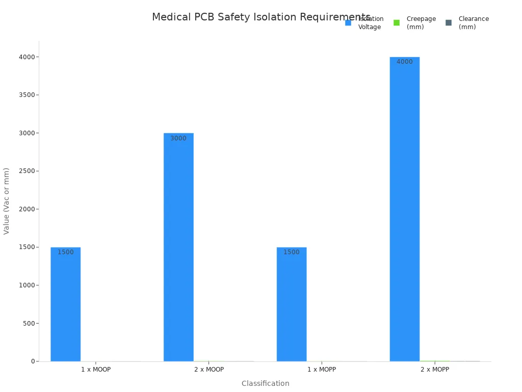
Rules like IEC 60601-1 tell you what these distances should be. You must pick the right insulation for your device. The table below shows what medical devices need:
Classifications | Isolation | Creepage/Clearance | Insulation |
|---|---|---|---|
1 x MOOP | 1500 Vac | 2.5 mm / 2 mm | Basic |
2 x MOOP | 3000 Vac | 5 mm / 4 mm | Double |
1 x MOPP | 1500 Vac | 4 mm / 2.5 mm | Basic |
2 x MOPP | 4000 Vac | 8 mm / 5 mm | Double |
You can see that higher safety needs bigger distances and higher test voltages. If you want reinforced insulation at 250V, your board must handle 4000V AC for one minute. This means you need strong materials and a careful layout.
Patient and Operator Protection
You keep patients and operators safe by following these rules. Good creepage and clearance stop dangerous currents from hurting people. You lower the chance of shocks and device problems. Here is why these distances are important:
Creepage and clearance stop electricity from jumping between traces.
They stop electrical arcing and leakage.
Following rules like IEC 60601-1 keeps your device safe and trusted.
You should always check these distances when you review your design. If you skip them, you put lives in danger and might fail safety tests. Good isolation helps you pass checks and keeps your good name.
Incomplete Risk Assessment in Medical PCB Design
Single Fault Conditions
You must always check for single fault conditions when you design a medical pcb. A single fault condition means one thing goes wrong, like a broken trace or failed component. If you do not plan for these faults, your device can fail in ways that hurt patients. You need to show that your design stays safe even if one part breaks. This is a key part of regulatory approval and compliance.
You should use different risk assessment tools to find and fix these problems. The table below shows the main techniques you can use:
Technique | Description |
|---|---|
Hazard and operability study (HAZOP) | You review each part of your design to find risks and weak spots. |
Failure modes and effects analysis (FMEA) | You list all possible faults and check how each one affects safety and function. |
Fault tree analysis (FTA) | You start with a bad outcome and work backward to find what could cause it. |
You need to document every risk you find. This helps you meet regulatory needs and pass compliance checks.
FMEA and Risk Management
You use FMEA to make sure your device stays safe and works well. FMEA stands for Failure Modes and Effects Analysis. This method helps you find every way your device can fail and plan how to stop it. You should follow these steps:
List every single-point failure in circuits that touch the patient. Write these in your risk file for regulatory compliance. Add extra vias or traces for important signals.
Test each backup part by making one fail on purpose. Check that your device still works right.
Keep your board clean. Make sure salt and halides are very low on every batch.
Plan for water or moisture. Use slots or special coatings for extra protection. Check coatings with UV light.
Use special finishes for BGA pads and make corner pads bigger.
Run high-temperature tests for long hours. Cut open some boards and check for cracks or damage.
Test for leaks after keeping the device in hot, wet air. Make sure current stays below safe limits.
You must keep records of all these steps. Good risk management helps you meet regulatory standards and keeps your device safe for patients.
Inefficient Thermal Management
Heat Dissipation Issues
You need to handle heat early in your medical device design. Too much heat can make the device stop working. It can also cause problems with how well it works. High-power ICs like processors, FPGAs, and PMICs make a lot of heat when running. Power circuits such as voltage regulators and DC-DC converters also get hot. If you do not control this heat, you can hurt sensitive parts. This can make your device not last as long.
Here are some common thermal management problems you might see:
Devices get too hot from bad part placement or missing thermal vias.
Hot spots can raise electrical resistance.
Heat stress can make solder joints weak and cause failures.
RF circuits may not work well if the temperature changes.
Tip: Try using thermal simulation tools to spot hot areas before you build your pcb. This helps you stop failures and keeps your device working well.
To fix these problems, you should:
Pick substrates that move heat away fast.
Place parts so they do not block each other’s heat.
Put thermal vias under parts that get hot.
Attach heat sinks to parts that heat up.
Use big copper planes to spread heat.
Match your layout to the way air moves in the enclosure.
Temperature Compliance
You must make sure your device stays within safe temperature limits. High temperatures for a long time can damage electronic parts. This can cause thermal runaway. Heating and cooling over and over can also break solder joints.
Follow these best steps to stay safe:
Use materials with a high glass transition temperature (Tg > 180°C) for stability.
Pick materials with a low coefficient of thermal expansion (CTE < 70 ppm/°C) to lower stress.
Make copper thicker to help heat move better.
Put lots of thermal vias near hot parts.
Add heat sinks or fans if you need extra cooling.
Make sure air flows well over heat sinks to stop hot spots.
Use wide power traces so more current can move safely.
You keep your device safe and working well when you fix thermal management problems. Good thermal design helps your device work right and pass rule checks.
Poor Material Selection for Medical PCBs
Biocompatibility Concerns
You need to pick biocompatible materials for medical devices. If you use the wrong materials, patients can get hurt. Some materials might react with body fluids or tissues. This can cause infections or allergic reactions. Every material that touches the body must pass strict safety tests.
The table below lists common biocompatible materials and their main features:
Material Type | Key Properties | Biocompatibility Status |
|---|---|---|
Polyimide (PI) | High thermal stability, flexibility, proven biocompatibility | Passed ISO 10993 testing |
Liquid Crystal Polymer (LCP) | Ultra-low moisture absorption, excellent barrier properties | Valuable for implantable devices |
PTFE (Teflon) | Chemically inert, hydrophobic, thermally stable | Suitable for rigid/mixed configurations |
Medical-grade coverlays | Protects circuitry, allows for laser ablation | Rated for ISO 10993 or USP Class VI |
You should always check if your materials meet ISO 10993 or USP Class VI. These rules help you show your device is safe for people. If you skip this step, your device could be recalled and patients could get hurt.
Tip: Ask suppliers for certificates for biocompatible materials. This makes audits and approvals easier.
Flammability Standards
You also need to think about fire safety when picking pcb materials. Medical devices are often close to patients and other equipment. If your materials burn easily, people can get hurt.
The table below explains the main fire safety classes:
Classification | Description |
|---|---|
V-0 | Burning stops within 10 seconds, no flaming drips allowed. |
V-1 | Burning stops within 30 seconds, no flaming drips. |
V-2 | Allows non-flaming drips, less strict than V-0. |
You should use materials that meet UL 94 V-0 for best safety. UL 796 and UL 94 are the main rules for printed wiring boards. These rules test how well your materials resist fire and electrical stress.
UL 796 checks if printed wiring boards are safe under stress.
UL 94 tests how plastics in your device burn.
If you follow these rules, you help keep patients safe and meet world safety standards.
Overlooking Testability and Inspection
Test Points and Access
You need to make sure your design allows for easy testing. If you skip test points or make them hard to reach, you risk missing defects. Good test point placement lets you check signals and power lines without damaging the board. When you add enough test points, you help inspectors find problems early. This step protects your product and your reputation.
If you do not include enough test points, you face several problems:
You cannot find all faults, which lowers your fault coverage. Most experts aim for 90-95% fault coverage in critical designs.
You may need to test by hand or skip electrical checks. This increases the chance of sending out bad products.
Defective units can reach hospitals or clinics, which can hurt your brand.
You should follow these best practices for testability:
Best Practice | Description |
|---|---|
Accessible Test Points | Place test points where you can reach them easily during inspection. |
Design for Testability (DFT) | Plan your layout so you can test and debug every part of the pcb. |
Automated Optical Inspection (AOI) | Use machines to spot defects early and improve quality. |
Tip: Work with your manufacturing team to document all test needs before you finish your design.
In-Circuit Testing Planning
You must plan for in-circuit testing from the start. This type of testing checks each part of your board while it is in place. In-circuit testing finds problems early and helps you avoid costly recalls. If you plan well, you can fix design flaws before they reach the customer.
Here are some key steps for strong in-circuit testing:
Add test pads for every important net.
Make sure probes can reach all test points.
Use a feedback loop between your design and testing teams. This helps you catch and fix issues fast.
The table below shows more best practices:
Best Practice | Description |
|---|---|
In-Circuit Testing (ICT) | Detects defects early and lowers recall risk. |
Continuous Feedback Loop | Lets design and test teams work together to solve problems quickly. |
Documentation of Test Requirements | Ensures everyone knows what to check and how to do it. |
When you plan for testability and inspection, you make your pcb safer and more reliable. You also meet strict medical standards and protect your business.
You keep patients and your business safe by avoiding medical pcb design mistakes. If you follow rules like FDA and ISO 13485 early, it is easier to get approval and lowers risk. Good records and risk checks help your pcb work well and stay safe. Learning new things and working with rule experts helps you keep up with changes and make better medical pcb designs.
FAQ
What is the most common mistake in medical PCB design?
Many people forget to check the rules early. This can slow down your project and cost more money. Always look at standards like IEC 60601 and ISO 13485 before you start.
How do you ensure traceability for medical PCBs?
You need to keep a record for each part you use. Use unique device identification (UDI) and pick suppliers who give you all the right papers. This makes it easy to track and recall devices if you have to.
Why is EMC/EMI testing important for medical devices?
EMC/EMI testing makes sure your device works safely near other electronics. You must pass these tests to meet safety rules and keep patients safe from device problems.
Which materials are best for biocompatible medical PCBs?
You can use polyimide, liquid crystal polymer (LCP), and PTFE. These materials pass ISO 10993 tests and are safe for medical use.
See Also
Essential Guidelines for Designing Effective PCB Circuit Boards
Key Skills Needed for Multi-Layer PCB Layout Mastery
Frequent Issues and Fixes in PCB Design for SMT
Ten Strategies to Reduce Expenses in Custom PCB Manufacturing
Seven Important Inquiries for Your PCB Manufacturer Pre-Production
