Multi-layer PCB Quality Inspection Key Points
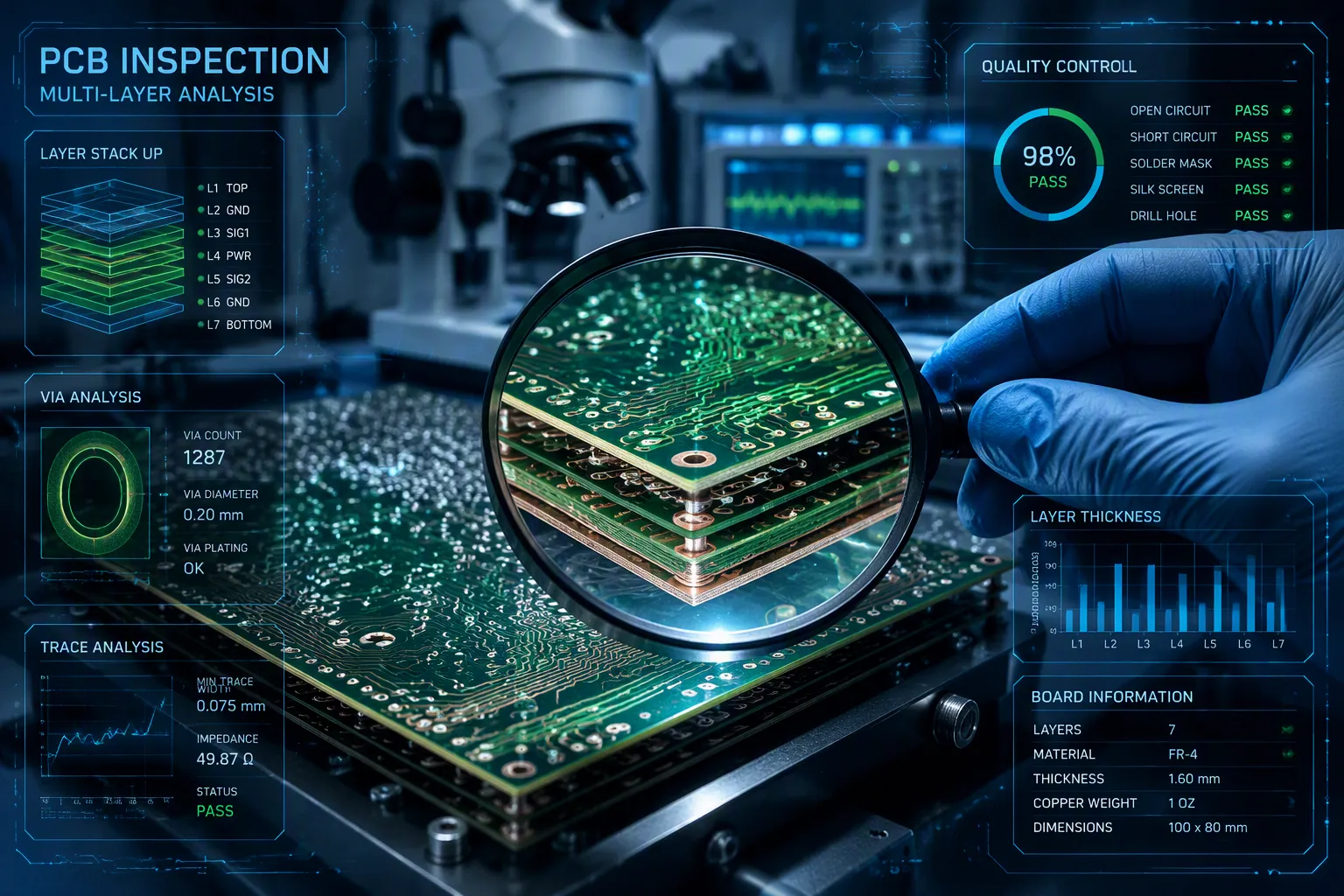
You cannot check a multi-layer PCB just by looking at its surface. After lamination, the inner layers stay hidden. Four methods fill this gap: automated optical inspection, X-ray inspection, electrical testing, and microsection analysis. Each method finds different kinds of defects, and together they protect product reliability.
Automated optical inspection, or AOI, is used the most in this field. AOI units made up 60% of automated inspection systems in PCB assembly lines, with over 14,500 units installed worldwide in 2024. These tools find surface defects on outer layers and inner layers before bonding. X-ray inspection then shows hidden flaws. Electrical testing confirms continuity. Microsection analysis reveals structural problems. Strong quality programs use all four methods and follow established standards.
Key Takeaways
Use four inspection methods together: AOI, X-ray, electrical testing, and microsection analysis.
AOI quickly finds surface flaws on inner layers before lamination.
X-ray inspection shows hidden problems, such as layers that do not line up and empty spaces in solder.
Electrical testing makes sure there are no broken paths and no unwanted connections, so the circuit works correctly.
Microsection analysis checks the inner layers and supports other inspection findings.
AOI for Multi-layer PCB
Automated optical inspection (AOI) helps you keep each multi-layer pcb at a good quality level. You use AOI to spot surface defects on inner layers before lamination. This step catches problems early in the process. Two topics matter in this section: how AOI performs inner layer inspection and what its limits are.
Inner Layer Inspection with AOI
Inner layer inspection begins with high-resolution cameras that scan each panel for faults. The cameras compare the board to a reference design. They look for differences between the two images. Inner layer inspection finds open circuits where a trace breaks. It finds shorts where two traces touch incorrectly. Missing pads are another target of inner layer inspection. The system flags improper trace width that can cause current issues. You depend on inner layer inspection for every critical panel. This inner layer inspection step happens before lamination seals the layers together. Proper inner layer inspection stops scrap from bad layers becoming embedded in the final board. You cannot skip inner layer inspection and still ensure final quality. Speed is a big benefit of this inner layer inspection approach. Each panel passes through the AOI machine in seconds. The system flags these defects for operator review. Inner layer inspection catches problems you would never see after lamination. The system records defect locations for later analysis. This defect detection process works best on clean surfaces.
Advantages and Limitations
AOI brings speed and accuracy to your manufacturing process. One machine can scan thousands of panels per shift. Defect detection rates for visible surface issues stay high. AOI supports inspection standards like IPC-A-600 for visual quality. This method improves overall product reliability.
However, AOI has key limits you must understand. AOI cannot examine the internal structure of a PCB layer. It cannot detect subsurface defects such as delamination or voids. After the lamination process, you can no longer use AOI for this task. Alternative methods like X-ray become necessary for post-lamination testing. You combine AOI with other methods to cover all defect types. This integrated approach protects your product integrity. Each method fills a gap that AOI alone cannot address.
X-ray Inspection for Multi-layer PCB
X-ray inspection can look through the board. This method uses X-rays to make pictures of hidden structures. You count on it when AOI cannot reach inside features. X-ray inspection shows misalignment between layers, voids in solder, and cracks in buried vias. These defects stay hidden from the naked eye. X-ray inspection works as a kind of non-destructive testing. You keep the board whole after the scan. This benefit makes X-ray inspection useful for costly or critical assemblies.
Detecting Internal Defects
X-ray inspection finds defects that form during lamination or assembly. Layer misalignment shows up as shifted copper patterns. Solder voids appear as dark spots inside joints. Buried via cracks look like thin lines inside the barrel. You catch these defects before they cause failures in the field. The imaging process shows the exact spot of each flaw. Operators then decide whether to scrap or rework the board.
X-ray inspection also helps find defects in dense multi-layer boards. High layer counts hide more inside features. The X-ray beam goes through all layers at once. You get a full picture of inside quality. This ability protects the integrity of complex designs.
Best Applications and Limitations
X-ray inspection works best when inside access matters most. You use it for buried vias, blind vias, and ball grid arrays. The method also helps with boards that have many layers.
Speed is the main drawback. The table below compares X-ray inspection with AOI.
Inspection Method | Speed per Standard PCB | Suitability for High-Volume Production |
|---|---|---|
AOI | Under 10 seconds | Ideal — scans thousands of components per minute, minimal line delays |
AXI (X-ray) | 30 seconds to 1 minute | Slower — detailed X-ray imaging and analysis slows throughput, especially for dense multi-layer boards |
Slower Processing: The detailed imaging process slows down production compared to AOI.
AOI gives speed and fits high-volume production. X-ray inspection is slower and costs more. Yet it gives unmatched insight into inside structures. This tradeoff matters for complex multi-layer boards. For high-volume manufacturing, the 30-second to 1-minute cycle per board limits throughput. You balance speed against the need for inside quality data. Many lines run AOI first and X-ray inspection second. This order keeps the line moving while still catching hidden defects.
PCB Electrical Testing for Quality
After AOI and X-ray check the board's shape, you test the electrical paths. Electrical testing makes sure each circuit path works. Two main methods are used: flying probe testing and fixture testing.
Flying Probe vs. Fixture Testing
Flying probe testers touch test points with moving probes. They do not need a custom fixture. You program the system from your CAD data and start fast. Fixture testing, or ICT, needs a custom bed-of-nails fixture. Each PCB design needs its own fixture.
The cost difference guides your choice. Flying probe costs nothing for fixtures. Fixture testing costs $3,000 to $50,000 for the first fixture. A batch of 1,000 boards costs about $5,000 with flying probe. Fixture testing totals about $4,167 including the fixture. At 10,000 boards, fixture testing cuts cost per board by 70 to 85 percent.
Test speed also varies. Flying probe takes 1 to 30 minutes per board. Fixture testing finishes in 5 to 120 seconds. New systems use 8 probes to test many points at once. They can reach up to 180 test cycles per second.
The break-even point is about 1,000 to 2,000 boards. Below that number, the fixture cost rules. Above that, ICT's faster speed pays off the fixture. Changing the program costs nothing. Changing a fixture may cost $500 to $5,000.
Continuity and Isolation Checks
Both test methods check two things. Continuity tests ensure each net has a full path. A broken trace means an open circuit. Isolation tests make sure no connection exists between separate nets.
Isolation testing measures resistance between networks. IPC-6012E requires at least 100 megohms of insulation for multi-layer PCBs. This standard makes sure conductors have enough space. Good isolation prevents signal problems.
These electrical tests find defects that AOI and X-ray miss. A tiny crack may pass visual inspection but fails a continuity test. A conductive particle between traces fails isolation checks. The four methods cover all key defect types. They make sure the board is structurally sound.
Quality electrical testing helps manufacturing reliability. One defect can make a board useless. Testing every panel keeps quality steady. You record results for tracking and meeting standards.
Microsection Analysis
Microsection analysis gives you the clearest view of a multi-layer pcb's internal structure. You cut a sample board, mount it in resin, and grind it down until the cross-section shows every layer. This destructive inspection reveals what no surface scan can show.
Process and Key Measurements
You polish the sample and view it under optical microscopy at approximately 50X to 500X magnification. This range lets you measure copper thickness, dielectric separation, and annular rings. You also spot delamination or voids. A calibrated measurement program reports dimensions with a 1–2 micron error margin. You verify results against IPC-A-600 for acceptability and IPC-6012 for dimensional specifications.
For via integrity, the via barrel must have no cracks. Barrel cracks are a common thermal-cycling failure mode. For HDI microvias, you check the microvia shape, depth, copper coverage on via walls, dimple depth, and void percentage. The microvia aspect ratio is generally limited to 1:1 for reliable plating and filling. Layer-to-layer registration is also measured, with the minimum annular ring on Class 3 external layers being 50 microns.
Inspection Item | Typical Evaluation |
|---|---|
Outer Layer Copper Thickness | Ensures required current capability |
Inner Layer Copper Thickness | Confirms multilayer structure reliability |
Hole Wall Copper Thickness | Verifies plating quality |
Via Copper Thickness | Ensures electrical connection stability |
Acceptance criteria per IPC-6012E: plated hole copper requires 20 µm average for Class 2 and 25 µm average for Class 3. Minimum annular ring is 50 µm for both classes. Dielectric spacing must be at least 90 µm for Class 2 and 100 µm for Class 3. Registration must stay within 100 µm for Class 2 and 75 µm for Class 3. IPC-A-600 also specifies that copper plating in vias must have no more than a 20% reduction in thickness at any point.
When to Use Destructive Testing
You cannot test every board this way. Microsectioning destroys the sample. You rely on quality control sampling instead. You pull panels at set intervals or after process changes. You also use it for failure analysis when a board fails electrical testing.
This method supports your manufacturing quality system. It confirms that plating, lamination, and registration meet standards. It also validates the other inspection steps. When aoi flags a defect, microsection analysis confirms the root cause. This combination builds reliability into every multi-layer board you ship.
Quality Standards for PCB
Standards give you a common way to judge a board. They turn unclear ideas like "good enough" into limits you can measure. Two documents matter most for multi-layer work: IPC-6012E for performance and IPC-A-600 for visual acceptance.
Adhering to IPC-6012E
IPC-6012E sets the lowest requirements for rigid printed boards. It defines copper thickness, annular ring width, and dielectric spacing for each class. For through-hole vias, the smallest annular ring is 2 mil (0.050 mm) on external layers and 1 mil (0.025 mm) on internal layers for Class 3. You check these values during microsection analysis and electrical testing.
When you follow standards like IPC-6012E, you protect both reliability and performance. A thin annular ring may pass a quick look. It can still crack after thermal cycling. The standard catches this risk before the board ships.
Establishing Acceptance Criteria
You need clear acceptance criteria for every inspection step. Visual inspection per IPC-A-600 is part of that set. Common visual checks include pits, scratches, and via presence.
Defect Type | Class 2 Acceptance | Class 3 Acceptance |
|---|---|---|
Surface scratches (general) | Acceptable if base laminate is not exposed and conductor integrity is not compromised | Rejectable if scratch depth exceeds 25% of conductor thickness |
Surface scratches (solder mask) | No base material exposed; no conductors exposed; no penetration greater than 50% of mask thickness | Same criteria apply |
IPC-A-600 surface condition criteria cover scratches, pits, nodules, dents, measling, crazing, weave exposure, and surface contamination. These visible defects are the most common cause of incoming QC rejection because they can be identified without magnification.
IPC-A-600 also lists acceptable levels for base material defects like scratches, dents, and foreign inclusions that could affect insulation characteristics. This adds to the acceptance criteria beyond just solder mask and conductor surface issues.
Your quality plan should tie each method to a standard. AOI handles surface defects. X-ray covers hidden structures. Electrical testing confirms continuity. Microsection analysis verifies structure. This approach keeps your manufacturing line consistent and your final product trustworthy.
HDI and Microvia Inspection
HDI and Microvia Challenges
HDI boards push inspection requirements further. Microvias connect layers through tiny holes. These structures create unique risks. Stacked microvias carry the highest risk. Each via sits directly on top of another. Many failure types appear in stacked configurations. The table below shows the main problem types you encounter.
Problem Type | Root Cause | Consequence |
|---|---|---|
Thermomechanical fatigue | CTE mismatch between copper plating and dielectric during thermal cycling | Target pad separation or barrel cracking |
Plating issues (voids/dimples) | Inadequate bottom-up copper plating in via filling | Stress concentrations in stacked vias |
Target pad separation | Strain concentrated along single vertical axis exceeding tensile strength of copper interface | Micro-crack formation leading to open circuit |
Misregistration | Top via slightly offset over bottom via | Laser drill damages underlying copper pillar edge, causing immediate plating failures or latent reliability issues |
You face these risks when designing dense multi-layer boards. Thermal cycling during operation creates stress. Copper and dielectric materials expand at different rates. This mismatch causes fatigue over time. Plating issues weaken the via structure. A small void can grow into a crack. Misregistration happens when layers shift slightly during lamination. Offset vias create weak points. You need specific checks to catch each problem. A single flaw can destroy board integrity.
Specific Quality Checks
You use a combination of methods for microvia checks. During production, cross-section analysis, AOI, and X-ray checks confirm quality. Cross-sectioning gives the most detail.
Follow this process for cross-section analysis of microvias:
Prepare the sample by cutting the HDI PCB perpendicular to the microvia and polishing the exposed cross-section.
Inspect the polished section under a microscope at 500–1,000× magnification.
Verify copper thickness uniformity by checking that the plated copper thickness falls within ±20% of the target value; this confirms whether the microvia copper deposition is acceptably uniform.
This method reveals plating voids, dimples, and cracks. You measure copper coverage on via walls. You check dimple depth and void percentage. The microvia aspect ratio stays limited to 1:1 for reliable plating.
AOI finds surface defects on outer layers. X-ray reveals internal misalignment. Together these methods support defect detection for HDI boards. You cannot rely on one technique alone. The combination ensures manufacturing reliability. Failure analysis uses cross-sectioning when problems appear. You cut into the failed board and examine the root cause. This data helps improve your process over time. Every microvia must meet the same standards.
You now see how four methods work together as one system. AOI catches surface faults on multilayer pcbs. X-ray finds flaws inside the board. Electrical testing proves continuity and isolation. Microsection analysis confirms the structure. Together they cover every important defect type.
Follow IPC-6012E and set clear acceptance rules for each method. This practice protects pcb quality and long-term reliability. No single inspection step does the job alone. The combined approach is your key to boards you can trust.
FAQ
Which inspection method should you use first?
Start with AOI. It scans panels in seconds. It catches surface defects on inner layers before lamination. X-ray, electrical testing, and microsection analysis come next. They cover hidden structures and electrical paths.
Can AOI replace X-ray inspection?
No. AOI cannot see inside a laminated board. It misses layer misalignment, solder voids, and buried via cracks. X-ray reveals these hidden defects. You need both methods for complete coverage.
How do you decide between flying probe and fixture testing?
Look at your production volume. Flying probe needs no fixture. It suits low volumes. Fixture testing costs more upfront but runs faster. The break-even point sits around 1,000 to 2,000 boards.
Why does microsection analysis matter if it destroys the board?
Microsectioning confirms what other methods cannot. You measure copper thickness, annular rings, and via integrity directly. Sampling at set intervals validates your pcb quality without testing every unit.
What standard should guide your acceptance criteria?
Use IPC-6012E for performance requirements. Use IPC-A-600 for visual acceptance. These standards define copper thickness, annular ring width, and dielectric spacing. They turn vague ideas about quality into measurable limits.
See Also
Mastering Quality Control Methods Throughout Printed Circuit Board Production Processes
Essential Knowledge Required For Designing Multi-Layer Printed Circuit Board Layouts
Seven Vital Quality Control Steps For High Current Heavy Copper PCB Assembly
Multi-Layer Circuit Board Production Processes And Prototyping Challenges Explained
Detailed Overview Of How Multi-Layer Printed Circuit Boards Are Manufactured
