Multi-material PCB Combined Manufacturing Process
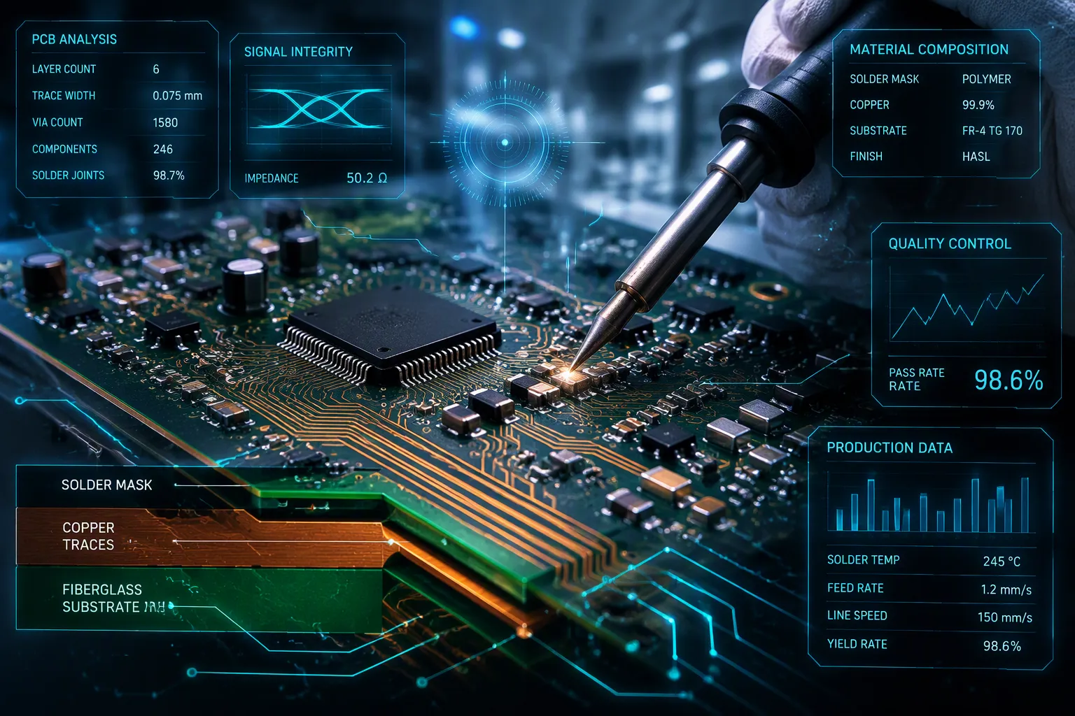
Do you need a board made from different materials? A multi-material PCB combines layers like FR4, polyimide, and Rogers into one stack. This stack design gives you custom electrical and heat-handling features. Making a multi-layer PCB takes careful planning. You must think about how each layer is built. The steps include pressing layers together with heat and pressure. You also control how much the materials expand to keep quality. This multi-layer PCB method is different from a standard PCB. Making a multi-material board needs exact work. The board’s build ensures it works reliably. The multi-layer PCB design boosts performance. You can use this method for RF circuits and hot environments. The final board meets many needs in one design.
Key Takeaways
Multi-material PCBs combine materials like FR4, Rogers, and polyimide to improve performance for high-speed and high-temperature uses.
Use low-loss materials for important layers to cut signal loss and improve heat control, while using standard materials in other areas to save money.
Watch the lamination temperature and pressure closely. This stops warping and helps layers stick together well.
Control thermal expansion mismatch by aligning CTE values and using high-Tg materials to prevent board warping and solder joint breakage.
Use plasma treatment to make different materials stick together better. This makes reliable boards that pass peel strength and thermal cycling tests.
Why Multi-material PCBs
Performance Benefits
High-speed signals need more than a standard board can offer. A multi-material PCB lets you adjust electrical properties for each layer. You can set the dielectric constant and copper weight with precision. This control gives you the characteristic impedance that high-speed interfaces require. Proper impedance matching stops signal reflections and ringing. Your data stays reliable and free from errors.
Insertion loss is very important at high frequencies. Different materials act in different ways. PTFE has the lowest loss at 0.15–0.25 dB per inch at 10 GHz. Rogers RO4350B comes next at 0.45–0.60 dB per inch. Megtron 6 reaches 0.55–0.70 dB per inch. Standard FR-4 loses 1.0–1.5 dB per inch at the same frequency. You can see the big difference. Picking a low-loss material for key layers keeps your signal strong. You save standard materials for parts that do not need as much. This mix gives you both performance and cost savings.
Thermal management also gets better when you choose the right materials. You put hot parts on layers that move heat well. The board pulls heat away from sensitive parts quickly. Your design stays cooler and lasts longer.
Common Material Combinations
You will see several common pairings in the industry. FR4 with Rogers laminates shows up often in RF designs. Rogers keeps stable dielectric properties at high frequencies. FR4 gives the board strength at a lower price. You use Rogers only where signals need its special traits. The rest of the board uses cheaper FR4.
FR4 with polyimide works well for hot environments. Polyimide handles extreme heat without breaking down. You might use this mix for aerospace or car electronics. The polyimide layers deal with the heat stress. FR4 layers give you the usual, low-cost base.
Another common mix is PTFE with FR4. PTFE gives you top-level high-frequency performance. Pure PTFE is hard to work with because it stays soft. Adding FR4 makes the structure more rigid. Your manufacturing becomes easier while keeping signal quality.
Each mix needs careful stack-up design. You must think about the coefficient of thermal expansion for every layer. The manufacturing process must handle different material behaviors. Your stack-up design directly affects yield and quality. A careful approach stops warping and delamination during fabrication.
Multi-layer PCB Manufacturing Process
Layer Preparation and Materials
Making a multi-layer PCB starts with getting each conductive layer ready. First, you pick your core materials. The inner core gives the board its shape and electrical traits. For regular designs, you choose FR-4. Its dielectric constant sits between 4.3 and 4.8 at 1 MHz. For high-speed uses, you pick Rogers. Rogers has a dielectric constant from 2.2 to 3.0 at 10 GHz. Its dissipation factor is 0.001 to 0.003 at 10 GHz, far lower than FR-4's 0.015 to 0.02 at 1 MHz. This steady value at high speeds makes Rogers great for RF circuits. You get even signal behavior across your working range. This early step in your PCB fabrication process sets the final performance.
You also need copper foil and prepreg. Copper foil comes in weights from 0.5 to 2 oz per square foot. It creates your conductive paths. Prepreg is a partly cured resin sheet. It joins layers together. You must match the prepreg's resin amount and thickness to your design needs. This matching gives proper dielectric traits and flow during lamination. Your stack-up design guides these material picks.
Now you get the inner layers ready. You put photoresist on a copper-covered core. UV light through a photomask hardens the resist in your trace shape. You wash off the soft areas. A chemical bath removes the extra copper. You strip the leftover resist. You check each layer for flaws.
Surface treatment comes after checking. You add a brown or black oxide coat. This makes a chemically active surface. The rough texture bonds well with the prepreg during lamination. This bond is vital for your multi-layer PCB strength.
Material | Role in Conductive Layer Preparation |
|---|---|
FR-4 | Core base for regular multilayer boards |
High-Tg materials | Core for designs needing more heat resistance |
Prepreg | Builds dielectric structure and bonds layers during lamination |
Copper foil | Forms conductive layers; thickness chosen per electrical needs |
Lamination, Drilling, and Plating
After prep, you move to lamination. You stack the inner layers with prepreg between each one. Alignment pins keep every layer in place. Misalignment over 0.1 mm can ruin the board. You apply heat between 170 and 180 degrees Celsius. Pressure goes up to 300 psi. The heat cures the prepreg. The pressure bonds all layers into one solid board. This lamination process needs close control. Temperature and pressure patterns must fit the materials in your multi-layer stack-up. Different materials cure at different speeds. You must control the ramp rate to stop uneven curing.
Drilling comes after lamination. You drill holes for vias and parts. The drill goes through different material hardness levels. You need sharp bits and exact speed control. You must set the drill speed and feed rate for each material type. The shift between layers needs careful setting changes. Your drill settings must match the multi-layer PCB stack-up.
Plating follows next. You use a chemical process to add copper inside the drilled holes. This links the different layers electrically. The copper bonds to the open edges of each conductive layer. Your vias carry signals across the whole board reliably.
You need quality checks all through the manufacturing process. Automated Optical Inspection scans for surface flaws. X-ray inspection finds hidden issues like voids in vias. For high-reliability boards, you do micro-section analysis. This checks plating thickness and layer bonding. Thermal stress testing makes sure the board handles temperature shifts without splitting. In-circuit testing checks electrical paths. Statistical Process Control watches solder joint height. If heights go beyond plus or minus 0.1 mm, the system warns you. You fix the issue right away to stop batch-wide defects. This quality focus keeps your multi-material PCB dependable.
Your multi-layer manufacturing process must handle each material's unique behavior. Different materials expand at different rates under heat. Your stack-up design must account for this difference. A good stack-up design stops problems before they start. The final result is a multilayer PCB that hits your performance targets. Every manufacturing step from material choice through final testing adds to success.
PCB Challenges and Solutions
Thermal Expansion Mismatch
Every material in your board expands when heated. The issue is that different materials expand at different rates. This difference creates stress inside your multi-material PCB. FR4 laminate expands 14–17 ppm/°C along its X-Y axis. Polyimide flex material expands 12–20 ppm/°C in the same direction. Those numbers look close. The real trouble appears in the Z-axis, the thickness direction. FR4 expands 50–70 ppm/°C there. Polyimide expands only 12–20 ppm/°C. This 3 to 5 times difference drives most thermal stress in a multilayer PCB.
Material | CTE X-Y Axis (ppm/°C) | CTE Z-Axis (ppm/°C) |
|---|---|---|
FR4 Laminate | 14-17 | 50-70 |
Polyimide (Flex) | 12-20 | 12-20 |
This uneven expansion causes two main problems. First, the board bends during heating and cooling cycles. The layers grow at different speeds, so the whole board bends. In bad cases, the layers separate inside the stack. Second, parts on the board can break. When a BGA sits on the board, the CTE mismatch between the board and the part creates stress on the solder joints. Each temperature change adds strain. Over time, small cracks form in the solder. The solder joints get tired and fail early.
You can handle this challenge in several ways. Match CTE values across your materials as closely as you can. This stops stress on copper parts during thermal cycling. Pick dielectric materials with high Tg, at or above 180°C, and low Z-axis expansion. These materials reduce stress from CTE mismatch. Use reinforced laminates with woven glass. The reinforcement makes the board stronger and less likely to bend. Keep lamination cycles between 2 and 3. Each cycle adds material shrinkage and CTE risks. More cycles reduce reliability and raise cost.
Your stack-up design must also deal with via reliability. Vias with low aspect ratio handle CTE mismatch easily. Vias with high aspect ratio focus stress in the middle of the barrel and at the neck. Repeated stress causes cracks at via necks in HDI boards. Thicker plating or via filling keeps a conductive path if a crack forms. Plan your stack-up with these risks in mind.
Adhesion and Reliability
Poor adhesion between different materials creates another problem. Non-polar plastics like PTFE do not bond well. Their surfaces repel water, so adhesives cannot spread evenly. You must treat the surface before lamination. Plasma treatment offers a good solution for this manufacturing process.
Oxygen plasma cleans dirt from metal surfaces. It adds polar groups like hydroxyl and carboxylic acids to the surface. These groups raise surface energy and water attraction. Adhesives spread and make good contact. This process can increase bond strength many times compared to old cleaning methods. Nitrogen plasma raises surface energy for polymers and composites. Argon plasma activates surfaces without oxidation, so it works well for metals. Hydrogen plasma reduces surface oxides for stronger bonds. Each plasma type helps with a specific bonding need in your multi-layer fabrication.
You must check adhesion quality with standard tests. Peel strength testing measures how well copper sticks to the substrate. The test uses a 90° peel angle at constant speed. The standard requires at least 1.1 N/mm per IPC rules. Failure means the foil separates or breaks. Thermal cycling tests check resistance to thermal stress. The profile runs from -40°C to +125°C for hundreds to thousands of cycles. No delamination, cracks, or via breaks may appear after inspection. Thermal stress testing puts the board in molten solder at 288°C for 10 seconds. No blistering or copper foil separation is allowed. These tests confirm your process makes reliable boards.
Peel strength data helps you pick materials. Results tell you how to prepare and roughen surfaces. Measured adhesion sets safe pad sizes and shapes for heavy parts. This quality focus stops delamination under real-world stress. Your fabrication process gets better with each data point you collect. The final multilayer PCB meets tough reliability needs across its whole life.
Multi-material PCB Applications
RF and Aerospace
Multi-material boards show up in many RF systems. The Rogers plus FR4 hybrid works well for several key uses. 5G networks use this mix for Sub-6GHz frequencies. You get solid performance without paying for a board made entirely of Rogers. Automotive radar and ADAS systems benefit too. You can put digital and RF circuits on the same board. This cuts down the number of parts and saves space. High-speed digital and IoT devices use the same method. You lower crosstalk and keep data safe in tight layouts.
Aerospace and defense need strict material properties. Your multi-layer PCB must soak up very little moisture. Humidity and altitude changes can cause reliability problems otherwise. You need stable dielectric properties for RF and microwave signals. Thermal conductivity pulls heat away from power-heavy parts. High Tg keeps the board stable at high temperatures. Low CTE lowers expansion stress during thermal cycling. Mechanical strength helps the board handle vibration and shock. Each need shapes your material choices and stack-up design.
Medical Devices
Medical implants put special demands on your PCB. Biocompatibility standards like ISO 10993 guide your material picks. USP Class VI and ASTM F1980 also apply. You choose polyimide substrates for flexibility and safe body contact. PTFE laminates offer dielectric strength and chemical resistance. Parylene coatings create a moisture barrier. Ceramic substrates provide hermeticity for neurostimulators.
Your manufacturing process must handle sterilization. Autoclaves, radiation, and chemical cleaning all stress the board. Your materials must survive repeated exposure without breaking down. You also design for long-term implantation. The board must work for 10–15 years inside the body. Thermal vias move heat away from sensitive areas. Redundancy and fail-safes protect patient safety.
Reliability testing is a must for medical devices. You run 100% electrical testing on every board. Burn-in testing catches early failures before implantation. Long-term reliability checks confirm the board lasts. You keep full traceability of lot numbers and manufacturing history. Regulatory audits need complete records. Your fabrication process must document every step.
The multilayer PCB approach gives you flexibility for medical designs. You combine rigid and flexible layers for complex shapes. This supports miniaturization in implantable devices. Your quality focus ensures each board meets strict standards. The result is a reliable product that serves patients safely.
Multi-material PCBs put several materials together in one board. You use them for fast signals, heat control, and small designs. Making them needs careful layer prep, controlled pressing, and exact drilling. You must handle how materials expand with heat and how they stick during the whole build.
These boards are getting more important as electronics shrink and speeds rise. New ideas will change how multi-layer PCBs are made:
Tiny microvias under 50 micrometers let you make very dense designs.
New dielectric materials make signals work better above 20 GHz.
Vacuum lamination pulls out air, which lowers voids and the risk of layers separating.
Low-temperature laminating materials let you add parts that can't handle high heat.
Your stack-up design choices directly affect how reliable the board is. This multi-layer method works for tough applications. Every multilayer PCB needs careful planning to make. Smart choices during manufacturing stop expensive mistakes. What material mix would you like to try for your next PCB design?
FAQ
What material combinations work best for high-frequency designs?
You can pair Rogers laminates with FR4 cores. Rogers keeps its dielectric properties stable at high frequencies. FR4 adds strength and costs less. This mix works well for RF circuits and 5G uses. Your multi-layer PCB design gets benefits from both materials.
How do you prevent warping during the lamination process?
You need to match CTE values across your materials. Pick dielectrics with high Tg, at or above 180°C. Set the lamination temperature between 170 and 180 degrees Celsius. Keep pressure at 300 psi. These steps lower stress during your multi-layer fabrication process.
What surface treatments improve adhesion between different materials?
Plasma treatment works best for non-polar materials like PTFE. Oxygen plasma adds polar groups to the surface. Nitrogen plasma raises surface energy for polymers. Argon plasma activates metal surfaces. These treatments help adhesives spread evenly and bond strongly.
How do you verify the quality of a multi-material board?
You run several tests. Peel strength testing checks copper adhesion, needing at least 1.1 N/mm per IPC rules. Thermal cycling from -40°C to +125°C checks resistance to stress. Thermal stress testing at 288°C for 10 seconds confirms no delamination occurs.
What stack-up design considerations matter most?
Your stack-up design must account for each material's expansion rate. Plan via aspect ratios carefully. Low aspect ratio vias handle CTE mismatch better. Keep lamination cycles between 2 and 3. Each cycle adds shrinkage and reliability risks to your manufacturing process.
See Also
How Printed Circuit Boards Are Fabricated Step By Step
Manufacturing Rigid Flex Multilayer Boards A Detailed Guide
Comprehensive Guide To Multilayer Circuit Board Production
Challenges In Prototyping Multilayer Circuit Boards Explained
Advanced Techniques For Manufacturing Heavy Copper Multilayer Boards
