The Importance of PCB Trace Width Calculation in PCB Design

PCB trace width calculation finds the exact size of copper lines carrying power on a board. Choosing the right dimensions plays a key role in modern PCB design. If you skip this step, thin traces act like resistors. High resistance creates unexpected voltage drops, causes too much heat to build up, and leads to sudden board failures.
You can easily prevent board burnout by sizing your copper paths correctly. Using standard IPC-2221 math formulas helps you find safe copper sizes for your power needs. You can also put your project numbers into an online trace width calculator to keep your circuits running safely.
Key Takeaways
Calculating the right trace width keeps the board from getting too hot and stops sudden circuit breakdowns.
Inside board layers need wider traces because trapped heat escapes very slowly.
Using thicker copper foil lets you use thinner lines to carry high electric power.
Online calculators use basic IPC-2221 math rules to find safe circuit wire sizes right away.
Trace Width Fundamentals and Failure Risks
Understanding PCB Trace Cross-Section
A board trace works just like a small 3D wire. Its total size depends on its width and thickness. You begin with basic copper foil thickness on the board, like 1 oz or 2 oz. Outside layers get extra copper added during the making process. Standard IPC-2221 rules ignore solder layers and secondary coatings when measuring final conductor thickness.
Layer Type | Base Material | Plating Added | Excluded Finish |
|---|---|---|---|
Internal Layer | Copper foil | Via plating (if present) | Secondary finishes |
External Layer | Copper foil | Plated copper through-holes | Solder coating / tin-lead |
A bigger trace size cuts down electrical resistance and makes less heat. Learning how trace width relates to power helps you build safe electronics. You can boost power flow by making traces wider or copper thicker. Inside traces trap heat inside the board material. Because of this, inner traces must be wider than outer layers to handle the same current safely.
Thermal and Electrical Failure Modes
Pushing too much electricity through a tiny copper line causes major issues. High power creates rapid heat spots inside the copper structure. This strong heat damages the bond holding the copper to the board in four clear steps:
High power density creates hot spots inside the copper trace.
Extra heat causes strong stress where copper meets the board base.
Thermal stress weakens the glue holding the copper to the board.
The copper trace peels off and lifts away from the board surface.
Constant heat raises board temperatures far past the standard safe limit of 10°C over room temperature. Using a trace that is too thin causes severe overheating and total board failure. You should always figure out proper trace sizes during design to stop power drops.
Wrong trace sizes mess up signal flow in fast digital circuits. Bad signal matching causes unwanted noise, bounce back, and lost data. This check is very important for high power projects. Good planning protects your circuit board from sudden breaks and costly damage.
Key Parameters in PCB Trace Width Calculation
Finding safe line sizes means you must balance a few physical details. Leaving out these main values causes big mistakes in pcb design. You must get correct numbers before starting any board layout math.
Maximum Current and Temperature Limits
You need to pick the safe power flow and extra heat limits for your circuit. Design current tells you the highest power your board trace carries safely. Passing more power through a trace requires a wider line to prevent dangerous heat.
Temperature rise is how much extra heat the trace can add above room air. Accepting a higher heat limit lets you use a thinner trace size. Many builders stick with a simple safety limit of 10 °C over room temperature. Running your board in cold places lets you pick higher heat limits.
The balance of trace width vs. current shows how heat shapes line sizes. Picking the right sizes keeps your circuit running safely under any working conditions.
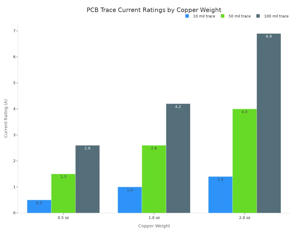
Copper weight | 10 mil trace | 50 mil trace | 100 mil trace |
|---|---|---|---|
0.5 oz | 0.5 A | 1.5 A | 2.6 A |
1.0 oz | 1.0 A | 2.6 A | 4.2 A |
2.0 oz | 2.0 A | 4.0 A | 6.9 A |
The standard table above shows safe current limits for outer board lines at a 10 °C heat rise. Allowing more heat lets the lines carry higher current safely. For instance, a 1.0 oz copper line with a 100 mil width handles 4.2 A at a 10 °C rise, but it takes 6.0 A at a 20 °C rise. You must check trace width vs. current balances early to keep your board safe from bad heat damage.
Copper Thickness and Layer Location
Board makers show metal thickness as weight per square foot of area. Spreading one ounce of copper across one square foot creates a basic metal thickness of 1.34 mil or 34.1 µm. Half-ounce metal gives 0.671 mil thickness, while two-ounce metal gives 2.68 mil thickness.
Picking thicker metal builds up the trace area very quickly. Using thicker metal lets you draw thinner power lines for high current flow. For example, a 1 oz copper line taking 3 A at a 10 °C heat rise needs a 110 mil pcb trace width. Adding extra metal thickness lets you shrink that main line width by a lot.
Where you put the line also changes how fast heat leaves the board. Outer surface lines cool off fast by letting heat escape straight into open air. Inside lines stay trapped right inside insulating board layers. Heat from buried lines must slowly pass through solid board stuff to leave, making a hard heat trap.
Because of this heat trap, inner board layers need much wider power lines:
Outer surface lines cool down quickly by releasing extra heat straight into open air.
Inner board lines must be about 2.5 times wider than outer lines to carry equal power at a 10 °C heat rise.
A 1 A line needs a 10 mil width on an outer layer, but it takes a 25 mil width on an inner layer.
Surface board layers handle high power lines much better, while inner layers shield faint data lines from bad signal noise.
Always re-check your trace width vs. current math every time you move lines to different board layers.
Standardized Calculation Methodology
Designing circuit boards does not require any guessing about copper line sizes. Industry guidelines offer clear math formulas to calculate exact trace dimensions. The IPC-2221 standard uses a simple formula to link electrical current, temperature rise, and cross-sectional area.
Standard IPC-2221 Calculation Formulas
The IPC-2221 guide explains how much electricity a copper path carries before it gets too hot. You find the needed cross-sectional area A in square mils with the formula A = (I / (k × ΔT^0.44))^(1/0.725). Here, I represents your current in amps, and ΔT is the allowed temperature rise in degrees Celsius. The placement factor k is set to 0.048 for outer layers and 0.024 for hidden inner layers.
IPC-2221 expresses current capacity as
I = k × ΔT^b × A^c, whereIis current in amperes,ΔTis the permitted temperature rise in °C,Ais trace cross-sectional area in square mils (width × thickness), andkis approximately0.048for external layers or0.024for internal layers.
Once you know the area, you turn that number into a physical pcb trace width. Standard one-ounce copper measures 1.378 mils thick. Dividing the total area A by this thickness gives you the necessary width in mils. Next, multiply by 0.0254 to convert those measurement values into millimeters. Choosing thicker copper foil lets you change your final line width. Knowing the right minimum trace width prevents dangerous overheating on your circuit board.
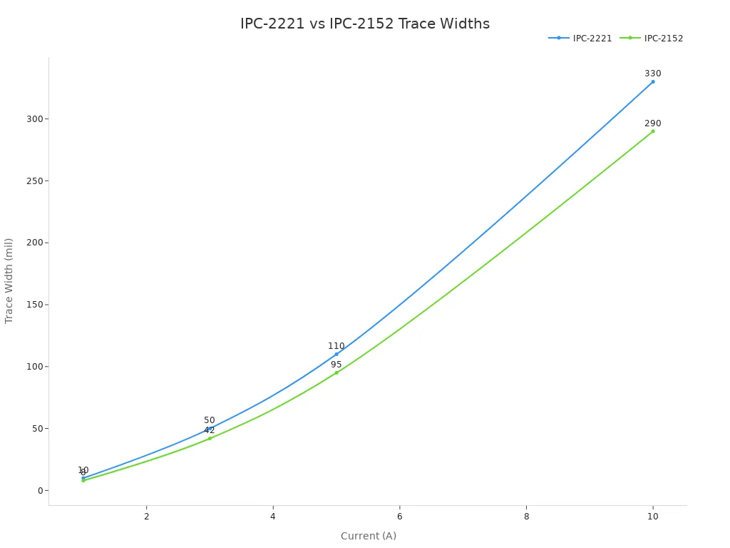
Aspect | IPC-2221 | IPC-2152 |
|---|---|---|
Data era | Legacy empirical data from the 1950s | Modern test and simulation data |
Document focus | General PCB design standard | Dedicated current capacity standard |
Method | Simple formula and charts | Charts plus correction factors |
Typical result | More conservative trace widths | Usually narrower, closer to real board behavior |
Ease of use | Faster for quick estimates | Better for detailed design decisions |
Engineers often check IPC-2221 values against the updated IPC-2152 standard. The newer IPC-2152 rules rely on modern heat tests that suggest slightly thinner traces. Even so, evaluating your trace width vs. current math with IPC-2221 gives you a safe safety buffer. This simple step keeps your line dimensions safe while the board works.
Using the IPC-2221 Trace Width Calculator
Math by hand takes time, so using a web calculator speeds up board design work. An online tool runs these standard formulas for you instantly. This makes it easy to review trace width vs. current numbers before building your circuit board.
Follow these simple steps when calculating trace width with an online program:
Type in your continuous design current using amps.
Enter your allowed heat increase, like 10 °C or 20 °C over room temperature.
Choose your basic copper weight, which usually starts at 1 oz/ft².
Set your target line location to an inner or outer layer.
Read the final results screen to find your required width in mils and millimeters.
The web calculator manages all the difficult math formulas automatically. The tool also shows line resistance, voltage drops, and power loss across your board. Checking your trace width vs. current early keeps your board reliable, safe, and ready for manufacture.
Practical Design and Routing Tips
Managing High Current Voltage Drops
You need to plan main power paths early when making a circuit board. Early size calculations give you a good start. Still, real board layouts create tight spots near pads, fuses, and parts. You must check these tiny areas to stop bad heat spots. Splitting power paths from thin sense lines using Kelvin connections helps you get correct voltage numbers on resistors.
Big copper shapes give electricity an easy path when one line is too small. Solid power layers lower resistance across your entire board. You can check your trace width vs. current numbers to keep power losses small. For big power projects, picking a wide line size stops major energy loss before making your real board.
Thermal Vias and Heavy Copper Sizing
Heat vias work like small cooling pipes right under hot parts. Adding a grid of open vias along your line path draws heat far away from top pads. For example, a 16 A trace uses big vias on both outer layers to spread heat fast. This clean setup moves part heat right into big ground layers.
Copper Weight | Minimum Spacing |
|---|---|
1 oz | 3.5 mil |
2 oz | 8 mil |
3 oz | 10 mil |
4 oz | 14 mil |
Using thicker metal lets you make your lines much thinner. Builders call copper heavy when it hits 3 oz/ft² or more on any layer. Pick heavy copper when a line carries over 50 A or works in rooms hotter than 85°C. Heat tests show basic 1 oz copper with thin coating breaks in 32% of boards, but 2 oz metal drops breaks down to 0.57%. You must use wider line gaps, like the chart shows, when picking thicker metal. Reviewing trace width vs. current math keeps your board working well. For huge loads over 100 A, solder thick metal bars right onto your board. Using good line sizes and thick copper keeps your board safe from heat damage. One last size check ensures great results.
Calculating the right pcb trace width protects your circuit board from dangerous overheating and sudden power drops. Safe pcb design always requires careful planning long before board manufacturing. First, identify your exact current needs. Next, select an allowable temperature rise for your working environment. Finally, consult IPC standards to confirm your physical dimensions and review all layout constraints.
You can easily prevent costly board failures with simple habits. Routinely run an online trace width calculator to verify your copper paths early in the layout process. Relying on a verified calculator and standard formulas keeps your electronic projects safe, functional, and ready for production.
FAQ
Why do inner layers need wider copper paths than outer layers?
Inside layers trap heat within the board material, which makes cooling very slow. Outside layers touch open air, so they cool off quickly. Because of this, you must draw wider inside paths to stop heat damage.
What happens if you pick a power trace width that is too small?
Lines that are too small act just like high-resistance resistors. High resistance creates bad voltage drops across your board layout. This extra heat weakens the glue and peels the copper right off the surface. Thin paths will burn out your project fast.
Should you use IPC-2221 or IPC-2152 for trace width estimates?
Using IPC-2221 gives you a quick math answer with a helpful safety margin. The IPC-2152 rule relies on new heat tests, which gives thinner lines. New builders like IPC-2221 rules because they keep circuits extra safe.
How does an online calculator help your pcb design?
A web calculator works out tough math formulas for you right away. You just type in your current, allowed heat rise, and copper weight. The tool changes these numbers into safe sizes, saving you time during pcb design.
Can a calculator estimate voltage drop and power loss?
Yes, a web tool calculates line resistance, full voltage drop, and power loss. Running these checks early stops surprise power bugs before you send the board out.
See Also
Essential Safety Guidelines And Precautions For Effective PCB Design
Understanding High Speed PCB Design And Its Critical Importance
Solving Frequent SMT Assembly Challenges In Modern PCB Design
Key Skills You Need For Multilayer PCB Layout Success
Crucial Design Strategies For Manufacturing Reliable High Density PCBs
