AI Server PCB Manufacturing Process Optimization
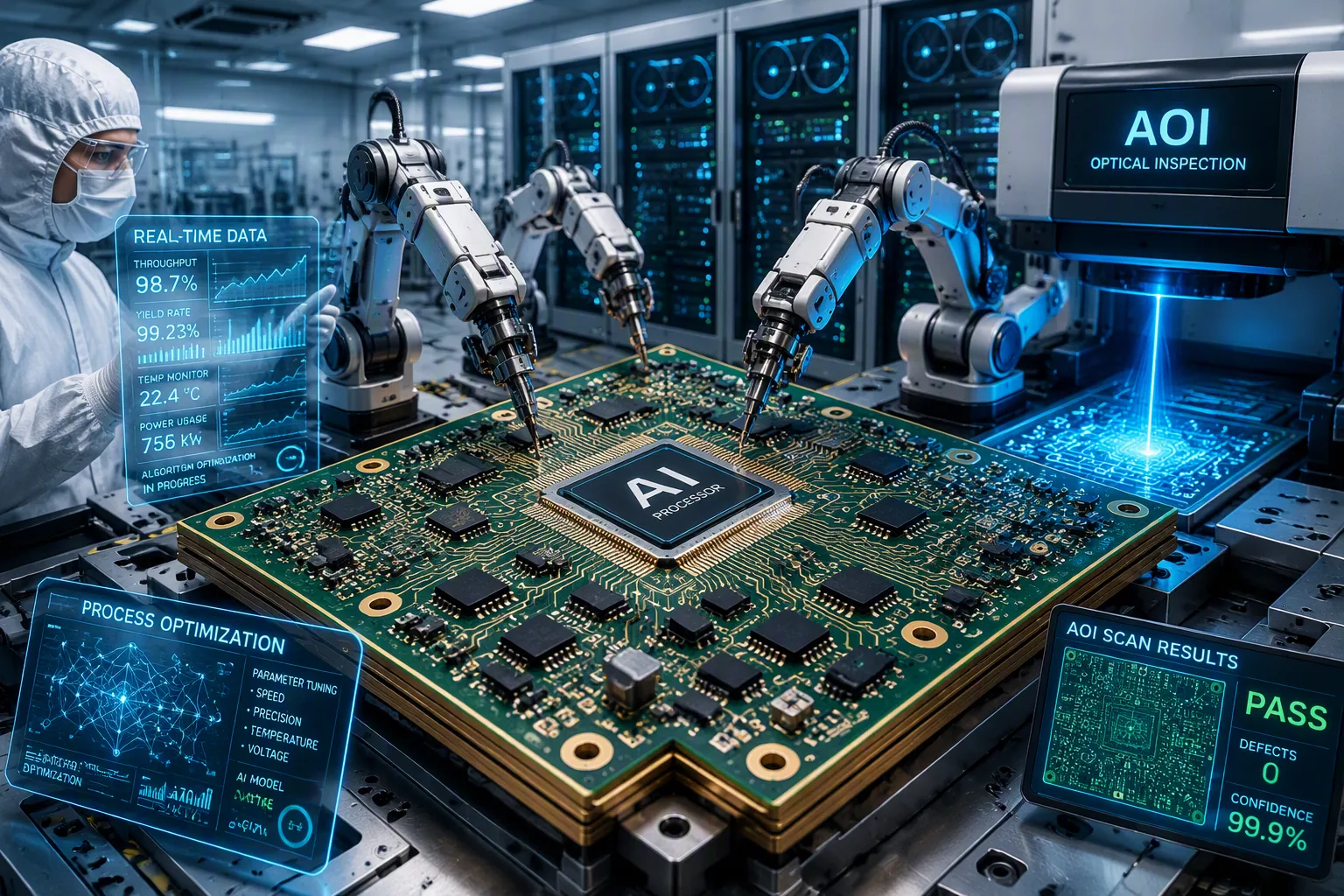
How can you make AI server PCB manufacturing work for extreme computing needs? Normal PCB methods are not enough for AI hardware. A regular PCB has 4–6 layers. An AI server PCB needs 20–32 layers. Each extra layer adds risk. You must control stackup, lamination, and drilling more tightly.
This work covers materials, design, making, and quality checks. Pick materials that work with your current production steps. That match drives growth and cost savings. Without it, you cannot scale up.
Thesis: This article explains key improvement areas—from choosing materials to AI-based quality checks—that allow steady, high-yield output. You will see how to raise performance, handle power, and cut waste. Your hardware, circuits, and server systems all gain from these steps. AI tools help spot flaws and boost yields. Power control and heat management stay major issues. Improvement touches every circuit layer and every server part you build.
Key Takeaways
Choose low-loss materials like Megtron 6 to keep signals clear and fast.
Use HDI design with microvias and fine traces to pack more power in less space.
Add thick copper and thermal vias to manage heat from powerful AI chips.
Let AI inspect boards with X-rays and optics to catch tiny flaws early.
Speed up prototyping with quick-turn services that match your production line.
Material Selection for AI Server PCB Manufacturing
The material you pick affects everything that comes after in AI server PCB making. You cannot fix signal loss or heat buildup after the board is made. The right laminate stops these problems before they start. You also need materials that work with the machines you already have. That matching decides if you can grow and keep costs low.
Low-Loss Laminates for Signal Integrity
Signal quality depends on two material properties: dielectric constant (Dk) and dissipation factor (Df). Dk measures how much a signal slows down in the material. Df measures energy lost as heat. Standard FR4 has a Dk of 4.3-4.8 and a Df of 0.015-0.020. Those numbers do not work for AI server PCBs. High-speed channels need Dk around 3.5-3.7 at 10 GHz. They need Df between 0.010 and 0.012. Low-loss materials like Megtron 6 or Megtron 7 meet these goals.
You should aim for a stable Dk range of 3.0-3.7 with very little change across frequency. Keep the change within ±0.05-0.1. That steadiness keeps the impedance the same. For dissipation factor, aim for values at or below 0.0025 for 112G or 224G channels. Rogers materials offer Dk of 2.2-3.0 and Df of 0.001-0.003. Those numbers look great. However, Rogers needs special RF processing lines. Most factories do not have that equipment. PPO-based laminates offer a better path. They work like FR4 in production. You can run them on standard multi-press sequential lamination tools. This choice avoids buying new machines. It directly lowers the cost per board and speeds up getting to full production.
Comparing insertion loss shows why material choice matters. Megtron 6 is the baseline. Tachyon 100G cuts insertion loss by 26%-43% over a 15-inch trace at 56 Gbps PAM4. At 16 GHz, Tachyon shows a 35% better loss profile. These improvements mean faster data transfer. AI server hardware needs speeds up to 112 Gbps per lane. Only high-frequency laminates with Dk below 3.5 and loss tangent below 0.005 can give that performance.
You should also think about glass weave and copper foil. Spread-glass laminates like 1067 or 1078 give even dielectric properties. They stop impedance problems. Very-low-profile copper foils such as HVLP or VLP2 reduce insertion loss from skin effect at high frequencies.
CTE and Thermal Conductivity Control
Coefficient of Thermal Expansion (CTE) mismatch creates serious reliability risks. Copper, laminate, resin, and solder mask all expand at different rates. Temperature changes cause uneven expansion. That stress leads to board warping, via cracking, and connection failures. Large AI server boards make this stress worse. Thin copper lines suffer the most. You must pick materials with matched CTE values. You also need balanced copper coverage across layers. This reduces stress during lamination and heat cycling.
High glass transition temperature (Tg) matters for thermal reliability. Aim for Tg of 170°C or higher. It is better to choose materials rated 180-200°C or above. Continuous work loads generate steady heat. Low Z-axis CTE stops via failure. Keep CTE below 50 ppm/°C below Tg. Above Tg, keep it within 200-250 ppm/°C. CAF-resistant laminates stop conductive anodic filament failures.
Thermal management needs careful design. Thermal via arrays under high-power ASICs use diameters of 0.3-0.5 mm. Spacing is 1-2 mm. These vias connect to copper planes that spread heat. Copper-filled vias give 20-30% lower thermal resistance than unfilled vias. Copper's high thermal conductivity makes this possible. This approach keeps junction temperatures within safe limits.
Standard FR4 gives thermal conductivity of only 0.3-0.4 W/m·K. That value is too low for AI heat loads. Aluminum substrates reach 1-3 W/m·K. Copper substrates achieve 5-10 W/m·K. Alumina ceramic provides 20-30 W/m·K. Aluminum nitride ceramic delivers 170-200 W/m·K. You need materials above the FR4 range for moderate heat zones. Ceramics handle critical hot spots. This thermal plan helps overall system efficiency.
Material compatibility with your current manufacturing processes remains your key lever. Choosing PPO-based laminates lets you use your existing setup. You avoid buying new equipment. You lower fabrication costs. You speed up time-to-market for high-layer-count boards. This approach makes high-performance PCBs possible without messing up your production flow. Every material choice affects circuit performance, power handling, and hardware reliability. Choose wisely at the start. Your whole manufacturing process depends on it.
HDI Design for AI Server PCBs
High-Density Interconnect (HDI) design changes how you approach AI server PCB manufacturing. Standard boards use through-hole vias that go through every layer. HDI boards use microvias, blind vias, and buried vias. These smaller parts let you route more signals in less space. For AI hardware, this density matters because processors pack thousands of connections into tiny areas.
High-speed signal integrity: Shorter connections, fewer via stubs, and finer details reduce unwanted electrical effects on high-speed serial, RF, and mixed-signal links.
Better routing can often lower total layer count, connector count, and overall system cost. HDI often lets you combine two or more regular PCBs into one board, making assembly simpler.
Fine Line Etching for Impedance Control
Fine line etching creates the narrow traces that carry high-speed signals. Standard PCB processes make traces wider than 150 microns. HDI manufacturing reaches trace widths of 25–50 microns. This difference changes everything about your circuit board design.
Parameter | HDI Specification | Standard PCB Specification | Benefit for Routing Density |
|---|---|---|---|
Microvia Diameter | 0.10–0.15 mm | >0.3 mm | Smaller vias allow more connections per area |
Trace Width | 25–50 microns | >150 microns | Narrower traces enable routing more signals |
Via Types | Blind, buried, microvias | Through-hole only | Layer-specific vias reduce signal path length |
You must control impedance precisely on these narrow traces. AI server PCB designs demand consistent impedance across every differential pair. Etching uniformity determines whether you hit that target. If one trace ends up wider than its neighbor, the impedance shifts. Signal reflections appear. Data errors follow.
The etching process requires tight tolerances. You need uniform copper thickness across the panel. You need consistent etch rates from board center to board edge. Any variation creates impedance mismatches that degrade performance at 112 Gbps speeds.
Via-in-Pad and Stack-Up Symmetry
Via-in-pad technology solves a major routing problem. Standard dogbone escape routing requires a short trace from the pad to a nearby via. This approach wastes space. Via-in-pad places the via directly inside the component pad.
Feature | HDI Capability | Impact on Routing Density |
|---|---|---|
BGA Pitch Handling | Supports 0.4 mm pitch (GPU/CPU) and 0.355 mm pitch (HBM memory) | Enables direct routing of advanced packages |
Via-in-Pad | Saves about 40% space compared to dogbone escape routing | Provides more room for traces and components |
Microvia Dimensions | Diameter ≤150 μm, depth ≤0.15 mm | Allows dense via placement, reduces signal loss by >30% |
Stack-up symmetry matters just as much. You must balance copper distribution across every layer pair. Unbalanced stackups cause warping during lamination. That warping shifts layer registration. It creates open circuits and short circuits. For a multi-layered PCB with 20–32 layers, symmetry becomes critical.
Your stackup also affects power delivery. AI hardware draws massive current at low voltages. You need dedicated power planes close to the processor. You need ground planes next to signal layers for return current paths. This setup controls impedance and reduces noise. The right stackup balances signal integrity, power integrity, and thermal management in one design.
Shorter signal paths from HDI construction reduce reflection and crosstalk. Blind and buried vias remove through-hole stubs that cause signal distortion. These benefits make HDI the right choice for AI server hardware that needs maximum performance from every circuit.
Advanced Fabrication for Thermal Management
AI server hardware creates a lot of heat. The NVIDIA H100 uses up to 700W of power. Normal fabrication methods cannot handle this load. You need better lamination, drilling, and plating methods. These keep your pcb safe under constant heat stress. Your manufacturing steps must change to meet these needs.
Copper Thickness and Buried Via Technologies
Thick copper layers add thermal mass. Layers above 3 oz carry more current and spread heat across the pcb. The NVIDIA A100 SXM Module uses a 14-layer Megtron 6 stack-up with a thick copper core under the die. This design keeps the GPU rail at 1.53V with less than 3mV droop during full-tensor operations. You get steady power delivery and better heat spread. Your circuit design gains from this.
Several key methods help you handle heat in high-layer-count boards:
Thermal vias move heat between layers
Large copper planes spread heat across the board
Heavy copper areas add thermal mass and conductivity
Copper coins give localized heat release
High-Tg materials resist high temperatures without breaking down
Smart component placement lowers thermal hotspots
For the NVIDIA H100, you need a combined plan. Use an embedded copper block with a thermal via array. This drilling method lowers thermal resistance to 0.8°C/W. Your lamination process must use high-Tg materials rated at 170°C or higher. Thermal conductivity should hit 0.8 W/m·K or more. These materials stop delamination during high-power use.
Buried via arrays create vertical heat paths. Any-layer HDI with stacked microvias allows dense connections. An 18-layer board for autonomous vehicle sensor fusion uses stacked microvias and copper coins under the SoC. It survives temperature cycles from -40°C to +105°C. That reliability comes from careful thermal design.
Embedded Components for Heat Management
Embedded components change how you manage heat. You put decoupling capacitors directly into inner layers. This move saves 40% of surface area. You free up space for other thermal management features. Your server hardware gains from this extra room.
Component Type | Effectiveness |
|---|---|
Embedded decoupling capacitors | Save 40% surface area, freeing space for thermal features |
Micro-heat dissipation structures | More efficient than external heatsinks, integrated into multi-layer substrates |
These methods boost overall energy efficiency. You cut the need for active cooling. Your ai server pcb manufacturing gains from fewer fans. The ai-driven pcb fabrication process helps you improve component placement. You can simulate heat flow before building the board.
Your server hardware stays cooler. Power delivery improves. Performance increases. You create boards that handle the extreme demands of AI computing. AI tools help you study thermal patterns. Your AI server needs reliable pcb performance. Manufacturing quality decides success.
AI-Driven Quality Control with Failure Analysis
Quality control decides if your AI server hardware survives in the data center. Manual checks cannot keep up with 20–32 layer boards. Human eyes miss small defects. Rule-based systems fail on new problems. AI changes this completely. You move from catching defects after they happen to stopping them before they start.
Automated X-Ray and Optical Inspection
Automated inspection systems with AI algorithms spot flaws that human inspectors miss. These systems learn from thousands of images. They recognize patterns across layers, vias, and traces. The accuracy numbers show the results clearly.
Inspection Scenario | Reported Accuracy | Context |
|---|---|---|
Continual classification (200 images) | 98% | Replacing manual and rule-based inspection |
Classification (453 good, 11 bad images) | 100% | Replacing manual and rule-based inspection |
Object detection for multiple defects (259 images) | 99.62% | Replacing manual and rule-based inspection |
These results show what AI brings to your production floor. You cut manual labor a lot. You lower scrap and rework costs. Your team works on root causes instead of repetitive scanning. The AI system checks every board with steady attention. It never gets tired. It never loses focus.
X-ray inspection finds internal problems. Buried vias, inner layer registration, and copper thickness all need checking. AI algorithms analyze these X-ray images in real time. They find voids in plated vias. They spot misalignments between layers. They flag thin copper areas that might fail under heat stress. Optical inspection handles surface defects. Solder mask scratches, trace width changes, and component placement errors show up right away.
The real power comes from using both methods together. X-ray sees inside the board. Optical inspection sees the surface. Together, they give you full coverage. Your ai-driven pcb fabrication process gets smarter with every board you run.
TDR for High-Speed Validation
Automated inspection finds physical defects. Time Domain Reflectometry (TDR) checks electrical performance. This testing method sends a fast pulse down a trace. It measures reflections that happen when impedance changes. You compare those measurements against your design targets.
TDR testing follows a clear sequence:
Test and validate: Use TDR tools to measure impedance after manufacturing and verify that it matches your design specifications.
This step lowers risks and boosts PCB performance, ensuring the final product meets required impedance targets.
TDR and impedance testing on coupons confirm the characteristic impedance of the manufactured board. This testing works alongside AOI, X-Ray, and cross-section micrographs. The goal stays simple: make sure the fabricated board matches simulation intent and stays within tolerance bands for high-speed operation.
A European industrial automation customer needed a 10-layer PCB with 100Ω differential impedance. The manufacturer optimized the stack-up, simulated impedance before production, and verified every production panel using TDR testing. The finished boards met impedance tolerance requirements and passed all functional testing. This example shows TDR's role in validating impedance control for high-speed applications.
TDR also finds signal degradation issues that may not show up during initial simulations. Eye-diagram analysis and signal quality measurements complement TDR results. Together, these methods catch problems early. You avoid shipping boards that fail in the field.
Building an internal failure analysis database turns defects into opportunities. Every flaw you find becomes data. AI algorithms learn from that data. They predict where future defects might occur. They suggest process adjustments before problems get worse. This database grows more valuable over time. Your manufacturing processes improve continuously. Your server hardware gains reliability. Your circuit designs perform better. Your power delivery stays stable. This approach transforms quality control from a cost center into a competitive advantage. AI-driven technologies make this transformation possible. You build better boards. You ship faster. You win more business.
Quick-Turn Prototyping for Data Center Infrastructure
Speed defines success in AI hardware development. Data center infrastructure projects demand rapid iteration cycles. You cannot wait weeks for prototype boards when competitors ship products monthly. Quick-turn prototyping compresses your development timeline dramatically. This speed lets you test new designs, validate thermal solutions, and verify signal integrity before committing to full production runs.
Rapid Prototyping Cycles for AI Hardware
Your prototyping cycle determines how fast you reach market. Standard PCB fabrication takes weeks. Quick-turn services collapse that window into days. The table below shows typical lead times for different board complexities.
PCB Layer Count | Quick-Turn Lead Time |
|---|---|
2-4 Layers | 24 Hours |
6-12 Layers | 48 Hours |
14-24+ Layers | 72 Hours |
A 12-layer AI server sub-board using Megtron 6 laminates was fully verified and shipped within a true 48-hour turnaround. That speed confirms the tabulated lead time for that layer count. Your hardware team can iterate designs rapidly with this capability.
AI-driven design tools accelerate this process further. Virtual validation happens before physical prototyping. Simulation tools integrated with CAD allow "first-time-right" prototypes more often. You reduce guesswork and save costly iterations. AI compresses hardware prototyping into rapid iteration cycles. Simulation runs that took hours now take minutes. This speed enables real-time hypothesis testing.
Key Step in Rapid Prototyping Cycle | How It Reduces Time-to-Market |
|---|---|
AI-assisted schematic design | Reduces design iterations and DRC issues |
Auto component placement and routing | Gets layout 50-70% complete automatically |
AI-accelerated solvers for signal, power, thermal integrity | Reduces physical prototype iterations |
AI-powered copilot learning from previous layouts | Accelerates placement and routing quality |
Sierra Circuits fabricated an AI-designed board with 843 components and 5,141 connections using advanced HDI precision. They achieved a 3-day fabrication and 3-day assembly turnaround. This result demonstrates significant production lead time reduction.
Integration with Existing Production Lines
Quick-turn capability depends on material and process compatibility. You cannot switch materials between prototype and production runs. That change introduces new variables. Your prototype results become meaningless. Choose materials that work across your existing manufacturing processes from day one.
PPO-based laminates offer this compatibility. They run on standard multi-press sequential lamination tools. You avoid special RF processing lines. Your quick-turn prototypes match your volume production exactly. This consistency improves manufacturing efficiency and reduces risk.
Your circuit designs benefit from this approach. Thermal performance stays predictable. Power delivery remains stable. Signal integrity matches simulation results. The automation built into your production line handles both prototype and volume runs without reconfiguration.
This integration creates a seamless pipeline. You validate a design in 48 hours. You scale to volume production without process changes. Your server hardware reaches data center infrastructure faster. Your manufacturing processes stay stable. Your performance targets remain achievable. Quick-turn prototyping becomes your competitive advantage in the AI hardware race.
These five pillars—material selection, HDI design, advanced fabrication, AI-driven quality control, and quick-turn prototyping—directly address signal integrity, thermal management, and yield. Each one strengthens your server hardware and circuit reliability.
When demand explodes, quality becomes the differentiator. QA isn't a checkpoint anymore. It's a competitive advantage.
AI connects fragmented data from component movements, serialized boards, and quality results. This creates complete manufacturing histories. AI-based automatic programming reduces setup time. Deep learning lowers false call rates. Continuous AI learning improves inspection over time. These capabilities boost first-pass yield and production throughput.
The next wave of AI server performance depends as much on clever PCB manufacturing optimization as on processor design. Manufacturers who invest in these practices today will support tomorrow's data center infrastructure. Audit your current processes now. Adopt these strategies to improve energy efficiency, manage power, and build reliable hardware for the future.
FAQ
What makes AI server PCBs different from standard PCBs?
AI server PCBs need 20–32 layers. They require low-loss materials and tight impedance control. Your hardware demands these features for reliable high-speed performance. Standard PCBs with 4–6 layers cannot handle these needs.
Why does material selection matter for AI server hardware?
Low-loss laminates keep signal integrity for your server hardware. Materials with high thermal conductivity manage heat from high-power AI processors. Your board design depends on these choices. Compatible materials work with your existing production tools.
How does HDI design improve circuit performance?
HDI uses microvias and fine traces to route more signals. This design reduces signal loss. Your hardware benefits from shorter paths. Better power delivery improves your AI server PCB performance.
What role does AI play in PCB quality control?
Algorithms inspect X-ray and optical images to catch defects. They find flaws human inspectors miss. Your circuit boards improve with fewer defects. This quality control reduces scrap and rework for your server hardware and power systems.
How can you speed up prototyping for AI server PCBs?
Quick-turn services deliver prototype boards in 48–72 hours. Use materials compatible with your production line. This lets you test AI server hardware designs fast. You validate power delivery before scaling to volume.
See Also
The Complete Guide To Printed Circuit Board Production
Enhancing PCB Yield Rates Through Online Automated Optical Inspection
Ten Strategies For Reducing Expenses In Custom Circuit Board Fabrication
Achieving Excellence In Quality Assurance For Circuit Board Manufacturing
Utilizing Horizontal Electroless Copper Deposition In Circuit Board Fabrication
