HDI and Microvia Technology for PCB Stators
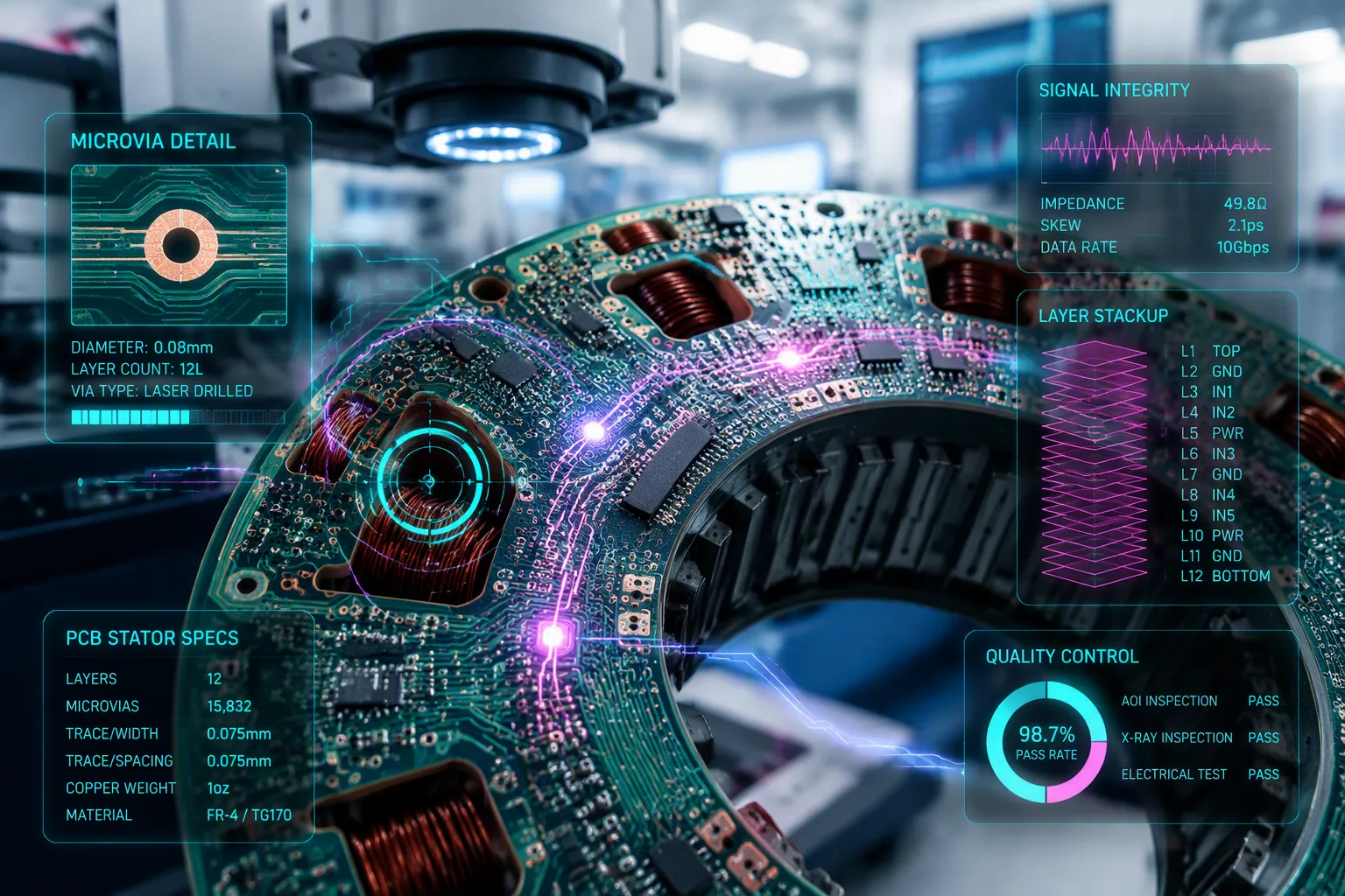
HDI and microvia technology lets PCB stators reach over 45% copper fill. This is much higher than the usual under 35% of regular designs. Microvias are laser-drilled through thin dielectrics. They allow fine-pitch routing. A 48-layer stator is built by stacking four 12-layer HDI modules. This HDI PCB stator prototype boosts torque and cuts volume. The HDI PCB stator setup also improves heat dissipation. Another HDI PCB implementation uses stacked vias. Yet another HDI PCB design reaches high density. Many PCB stators now use HDI and microvia technology. HDI allows miniaturization without losing performance.
The prototype motor is said to beat commercially available options. It gives higher torque at low speeds while taking up much less space.
Key Takeaways
HDI stators get more than 45% copper fill. This boosts torque and makes them smaller.
Embedded copper or aluminum coins draw heat away, helping stators stay cool and reliable.
Laser-drilled microvias and careful plating make strong connections without empty spaces.
24-layer PCB stackups give high routing density and steady signal integrity.
HDI and Microvia Technology Fundamentals
What Are Microvias and How Are They Formed
Microvias are small holes that connect layers in a pcb. Manufacturers create them using laser drilling. This process cuts through thin dielectric materials. The lasers make very small holes. These holes range from 0.075 mm to 0.15 mm in diameter. The small size allows designers to pack more connections into less space.
For reliable plating, microvias should not exceed a 1:1 aspect ratio. Designers calculate aspect ratio as dielectric thickness plus outer copper foil thickness divided by microvia diameter. A recommended target is 0.75:1 for reliable plating. Designers should avoid going below a 4-mil (0.10 mm) diameter. When laser drilling, copper foil thickness should not exceed 1/2 oz. Thicker foil creates ablation difficulties.
Laser drilling has depth limitations. The depth of focus restricts these vias to crossing a single layer in a thin dielectric. Manufacturers form longer stacked structures with multiple laser hits. This approach reduces misregistration compared to mechanical drilling. These features make microvias ideal for high-density designs.
Hdi and microvia technology enables dense interconnections. Designers rely on this technology for compact stator designs. An HDI pcb often uses microvias for this purpose. Designers use an HDI pcb stackup to combine many functions. This HDI pcb approach maintains signal integrity across layers. Another HDI pcb variant uses stacked microvias for vertical connections. Yet another HDI pcb design staggers microvias for reliability. Many designers choose an HDI pcb for complex stator applications. The HDI pcb construction supports high routing density. Each HDI pcb layer adds routing channels. A well-designed HDI pcb maintains impedance control. The HDI pcb format enables miniaturization without performance loss.
Standard HDI Build-Ups for Stator PCBs
The pcb industry has standardized build-up types for hdi. Type 2 follows a 2+N+2 structure. This means two microvia layers on each side of a core. Type 3 includes at least two microvia layers per side. These build-ups use blind and buried vias for layer connections. Blind vias connect an outer layer to an inner layer. Buried vias connect inner layers without touching outer layers. Designers also use stacked or staggered microvias. Stacked microvias sit directly on top of each other. Staggered microvias offset from one layer to the next.
An HDI pcb stackup can implement Type 2 or Type 3. Designers select an HDI pcb structure based on density needs. This HDI pcb approach allows complex interconnections. Sequential lamination builds each layer group separately. Sequential lamination creates each microvia layer one at a time. An HDI pcb requires careful sequential lamination planning. Another HDI pcb design uses sequential lamination for each pair. This process builds reliable vertical connections.
Blind and buried vias increase routing density. Designers achieve fine-pitch routing on an HDI pcb. High-density interconnection techniques enable this routing. The HDI pcb with HDI supports high-speed signals. Hdi and microvia technology provides the foundation for this performance. Designers maintain signal integrity through careful layer assignment. Impedance control becomes critical on an HDI pcb. Routing density increases with each additional layer pair. The HDI pcb stackup provides many reference planes. Each HDI pcb layer requires careful stackup design. The stackup design determines final performance characteristics.
Benefits of hdi for Stator Performance
Higher Power Density and Miniaturization
HDI technology gives stator performance clear, measurable gains. The copper fill rate goes past 45 percent, while standard designs stay under 35 percent. This higher copper density boosts torque output directly. A stator made with HDI can create more magnetic flux in the same space. Designers do this by fitting more turns and thicker copper into every layer.
Miniaturization comes naturally from higher density. An HDI PCB stackup swaps bulky wire windings for thin copper traces. The motor's overall volume shrinks while torque stays high or even grows. This matters for uses like robotics, drones, and electric vehicles. Every cubic centimeter of saved space can hold batteries or payload instead.
HDI also makes stators more reliable and easier to build. Laser-drilled microvias create connections that are precise and repeatable. Mechanical drilling cannot match this precision at small scales. The result is fewer defects and higher production yields. High-speed performance improves too. Shorter interconnect paths cut parasitic capacitance and inductance. Signal integrity stays strong even at elevated switching frequencies. Designers who need clean signal integrity across many layers depend on HDI stackups. Impedance control becomes manageable with dedicated reference planes in the stackup. These planes sit close to signal layers and steady the return path. For motor drive electronics, stable impedance control stops reflections and ringing. High-speed signal integrity is vital when gate drivers switch rapidly. HDI handles these fast edges without too much noise.
Thermal Management Using embedded coin technology
Heat is still a top enemy of stator performance. High current through dense copper creates big resistive losses. Traditional PCB materials let heat escape slowly. Embedded coin technology fixes this problem head-on. Manufacturers put a copper or aluminum coin into the PCB substrate. The coin sits under hot components or high-current traces. Heat moves through the coin and into an outside heatsink or chassis. Copper coins give excellent thermal conductivity. Aluminum coins offer a lighter, cheaper option. Both choices beat standard dielectric materials by a wide margin.
Embedded coin design considerations include coin placement, thickness, and bonding quality. The coin must line up exactly with heat-generating areas. Poor alignment wastes the thermal path. Thickness affects both heat capacity and mechanical fit. Bonding between the coin and nearby laminate must stay void-free. Voids trap heat and create hot spots. Designers also treat the coin as an internal heatsinks element. It spreads heat sideways before moving it upward. This spreading action lowers peak temperatures across the stator. Cooler operation extends insulation life and keeps torque steady. Engineers who weigh embedded coin design considerations early in the layout phase avoid costly redesigns later.
The mix of HDI routing and coin-based thermal management creates a stator that runs cooler, lasts longer, and fits into smaller spaces. These advantages build on each other. Denser copper means more heat, but better thermal paths remove it efficiently.
HDI Manufacturing Processes and Challenges
Laser Drilling and Copper Plating for Microvias
Making and plating a via starts with laser drilling. A UV or CO₂ laser cuts the microvia into the dielectric layer. Then desmear and cleaning take away leftover resin. Plasma or chemical methods get the via surface ready for metallization. A seed layer then forms using electroless copper or direct metallization. Bottom-up copper plating comes next. Pulse-reverse or controlled DC plating helps copper deposit more at the via bottom. This method fills the hole little by little and keeps voids low. Planarization makes the filled surface flat for later buildup. Pattern plating adds copper to build the outer circuitry.
Plating chemistry, current density, agitation, and leveling additives all need close control. Copper has to grow upward instead of closing the via opening too soon. Surface copper thickness and final dimple depth also need checking. The strong copper plug that results gives great electrical and thermal conductivity. Its CTE is very close to the copper metallization around it. This close match gives stacked microvias strong mechanical reliability. Copper-filled microvias beat non-conductive and conductive epoxy choices in thermal cycling. Voids act like stress points and speed up fatigue during interconnect stress testing.
Ensuring Reliability in Stacked Microvia Structures
Reliability testing checks that stacked microvias are solid. Interconnect Stress Testing per IPC-TM-650 Method 2.6.26 uses DC current to create thermal cycling. A 5% rise in resistance means failure. Thermal shock testing per IPC-TM-650 Method 2.6.7.2 puts microvias through fast temperature changes from -40°C to 260°C. These tests find weak spots before field deployment.
Design rules stop common failure modes. Interface failures between stacked vias come from different expansion during thermal cycling. Preferring staggered or offset placements and limiting layers per structure lowers this risk. Enforcing annular rings at least 50% oversize relative to via diameter adds more protection. Void-induced failures need pulsed plating and cross-sectional inspection. Neck fractures call for low aspect ratios and even plating thickness. Pad lift needs clean substrates and laminate materials that work well together. Using low-CTE resins in HDI cores and balanced, symmetric stackups keeps layer-to-layer registration tight. Designers who follow these rules protect routing density and signal integrity across every layer.
Advanced Stackup and Future Directions
Designing with a 24 Layer PCB Stackup
A 24 layer pcb stackup gives stator designers space for complex connections. Each layer pair adds routing paths without making the board thicker. The 24-layer pcb format keeps a thin shape even as layers increase. Designers use a 24 layer pcb stackup to keep power, ground, and signal layers apart. This separation helps strong signal integrity across the whole board. A 24 layer pcb also allows special planes for the power distribution network design. Those planes keep voltage steady for every gate driver and sensor.
Building a 24-layer pcb needs careful planning. Sequential lamination makes each microvia layer one at a time. A 24 layer pcb stackup must stay balanced to stop warping. Symmetrical stackup construction keeps copper weights and dielectric thickness equal on both sides. Designers follow hdi pcb design rules for via placement and aspect ratios. Controlled impedance traces need steady dielectric spacing on every 24-layer pcb. Impedance control shields fast switching edges from reflections. A 24 layer pcb stackup also supports high routing density in tight stator footprints. The 24 layer pcb approach fits high-layer-count designs. Each 24-layer pcb revision should record layer assignments clearly. A 24 layer pcb stackup rewards early planning during 24 layer pcb fabrication.
Comparing hdi Stators with Conventional Approaches
HDI stators are very different from traditional wire-wound designs. Wire-wound stators need copper coils wound by hand or machine. That process adds labor cost and limits slot fill. HDI stators use plated copper traces instead. An HDI PCB stator reaches over 45 percent copper fill, while wire-wound and standard PCB stators stay under 35 percent. Higher fill means more torque from the same volume.
Standard PCB stators fall between the two extremes. They cost less than HDI at low layer counts. However, they cannot match the routing density of an HDI pcb. HDI stators cost more upfront because of laser drilling and sequential lamination. Over time, HDI stators last better in the field. Their copper-filled microvias resist thermal cycling. Wire-wound stators suffer insulation breakdown and vibration damage. Standard PCB stators struggle with heat in high-current use. An HDI pcb spreads heat across more copper. Designers who weigh long-term field performance often choose HDI. The HDI pcb stackup delivers reliability that conventional stators cannot match.
An HDI pcb uses HDI and microvia technology for density. This HDI pcb improves thermal management. The HDI pcb offers design flexibility. Every HDI pcb needs manufacturing care. An HDI pcb pilot uses Type 2. This HDI pcb requires partner testing. The HDI pcb uses embedded coin technology. Each HDI pcb layer plans well. An HDI pcb maintains signal integrity. That signal integrity ensures stability. Another HDI pcb adds reliability. The HDI pcb supports complex routing. An HDI pcb saves valuable space. This HDI pcb validates performance gains. That HDI pcb succeeds. This HDI pcb design works. The HDI pcb fits stator needs. An HDI pcb delivers torque. The pcb test passes. Evaluate HDI for your next project.
FAQ
What HDI build-up should a designer pick for a first stator project?
A Type 2 build-up (2+N+2) works well for most first attempts. It places two microvia layers on each side of a core. Type 3 adds at least two microvia layers per side for denser routing. Designers should match the build-up to their routing needs and budget.
How small can a microvia get before plating becomes unreliable?
The article recommends a minimum diameter of 4 mils (0.10 mm). Designers should target an aspect ratio of 0.75:1 for reliable plating. Microvias should not exceed a 1:1 aspect ratio. Copper foil thickness should stay at or below 1/2 oz to avoid laser ablation problems.
Which materials work best for thermal management in high-current stators?
Embedded copper coins offer excellent thermal conductivity. Aluminum coins give a lighter, cheaper option. Both beat standard dielectric materials by a wide margin. Designers must align the coin with heat-generating areas and keep the coin-to-laminate bond void-free. Voids trap heat and create hot spots.
How do manufacturers test stacked microvia reliability?
Interconnect Stress Testing per IPC-TM-650 Method 2.6.26 uses DC current to create thermal cycles. A 5% rise in resistance signals failure. Thermal shock testing per IPC-TM-650 Method 2.6.7.2 cycles parts from -40°C to 260°C. These tests find weak spots before field deployment.
Do HDI stators cost more than wire-wound or standard PCB stators?
HDI stators cost more upfront. Laser drilling and sequential lamination drive the price. However, HDI stators last better in the field. Their copper-filled microvias resist thermal cycling. Wire-wound stators suffer insulation breakdown and vibration damage. Standard PCB stators struggle with heat in high-current use.
See Also
Analyzing Costs And Benefits Of Advanced HDI PCB Microvia Technologies
Explore Modern HDI PCB Prototype Methods Right Now
Essential Design Rules For Making Reliable HDI PCB Boards
Advantages Of LDI Exposure Machines For HDI PCB Circuit Production
Understanding Design And Manufacturing Of HDI Any Layer PCBs
