Tips for Optimizing HDI Microvia Design in 2026
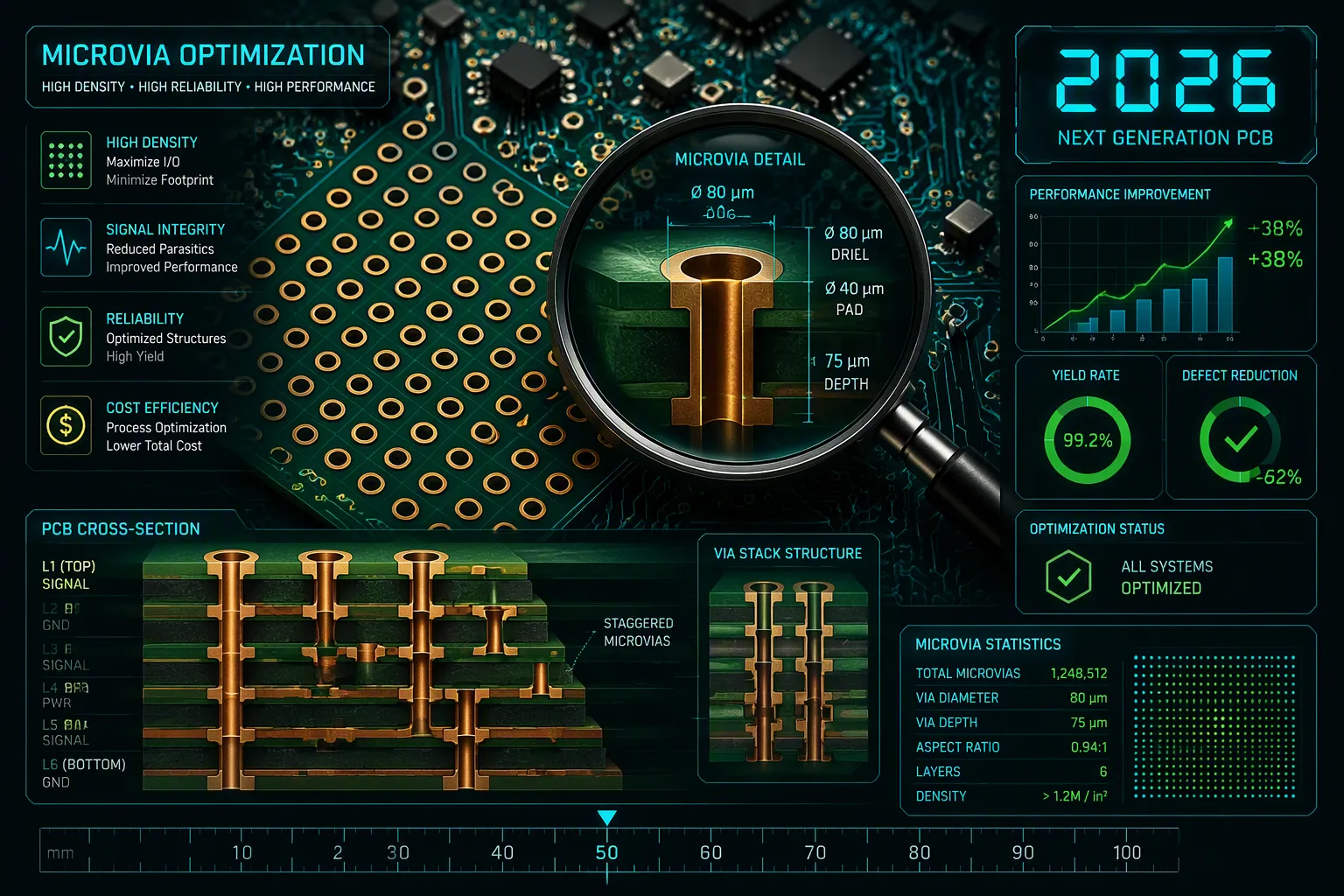
Your hdi microvia design decides how well your product works. The HDI PCB market will hit USD 21.26 billion by 2026, growing 8.5% each year through 2033. This growth comes from smaller parts, electric cars, and 5G. Improving your design helps signal quality, lowers costs, and boosts reliability. You need to learn the basics of via types and laser drilling. You also need simple rules for sizes and stack-ups. Advanced methods like via-in-pad boost high-speed performance. Good manufacturing steps keep your product dependable. Future changes will alter how you design HDI. This guide gives you clear steps for each area, from basics to future trends. Use these tips to stay ahead in 2026.
Key Takeaways
Make sure the aspect ratio is 0.75:1 or less so the plating works well.
For high-speed signals above 2 GHz, use via-in-pad to improve signal integrity.
Choose staggered vias instead of stacked vias. This gives you better reliability and costs less.
Choose low-loss materials with Dk below 4 to reduce signal distortion.
Always fill and cap microvias to stop solder problems.
HDI Microvia Fundamentals
Microvias form the backbone of modern high-density interconnects. These tiny holes measure 6 mils or less in diameter. Laser drilling makes these holes in thin material that does not conduct electricity. Copper plating joins two copper layers that are next to each other. This method puts more wires into less space. A board with microvias can hold six parts, while a regular board holds only four. Learning this HDI microvia design method makes the board smaller and improves signal quality for HDI boards.
Types of Microvias for High-Density Interconnect
Learn five microvia types for your HDI projects. Blind microvias begin on the top layer and end one layer down. For two-layer links, use stacked or staggered types. Buried microvias are inside the board and do not touch the top or bottom. These vias need copper filling and plating without gaps. Stacked microvias line up straight through many layers. They are reliable only up to two layers. Staggered microvias are placed sideways between layers. They are easier to make and more reliable than stacked ones. Skip microvias go through several layers but skip one middle layer. Fill them with epoxy to stop solder from flowing away.
Laser drilling makes these microvia structures on circuit boards. Laser systems make holes as small as 0.05 mm (50 microns). A standard microvia has a 0.1 mm size and a 1:1 depth-to-width ratio. Advanced laser systems drill up to 9,000 vias each second. They control depth very accurately, less than 0.25 mm per pass. This accuracy improves signal quality by cutting down on via stubs and lowering unwanted capacitance. Laser-drilled vias handle signal speeds over 10 Gbps and reduce electromagnetic interference.
Benefits of Microvias in HDI PCBs
Microvias give two big benefits for your PCB designs: better signal quality and smaller size. Shorter paths for signals reduce signal loss. Less unwanted capacitance and inductance make circuits work better. Less crosstalk and electromagnetic interference come from good HDI signal routing.
Smaller size drives the use of microvias in many industries. You can add more layers without making the board bigger. This allows complex designs in small smartphones and IoT devices. More parts per area means more features in a smaller space. This density of connections is important for PCB uses.
Staggered vias are easier to make and more reliable than stacked vias. For reliable plating, the microvia depth-to-width ratio should not be more than 1:1; larger ratios cause plating defects.
Key Design Rules for HDI Microvia Design
Now you need to apply the basics to real design rules. These rules guide your choices for via size, pad size, and aspect ratio. They also help you set up your stack-up for high-density interconnect routing. Follow these guidelines for your HDI PCB design to get reliable performance and cost-effective results.
Via Size, Pad, and Aspect Ratio Guidelines
The first step is to pick the right via diameter and pad size to support fine lines and spaces. IPC-2226 defines microvias with diameters between 50 and 150 µm. The recommended production range for reliable laser-drilled vias is 75–150 µm. The aspect ratio is the dielectric thickness plus copper foil thickness divided by the via diameter. For high reliability, keep the aspect ratio at 0.75:1 or lower. The limit is 1:1 for laser drilling. Larger ratios increase the risk of plating defects and reflow cracks.
The table below summarizes the key parameters for 2026.
Parameter | Guideline (2026) |
|---|---|
Via diameter | 75–150 µm (production range) |
Recommended aspect ratio | 0.75:1 to 0.8:1 |
Pad size | 0.25–0.30 mm for 0.10 mm via |
Dielectric thickness (L1-L2) | Typically 60–80 µm |
The pad size formula is critical. For a 100 µm laser via with a target residual ring of 40 µm and a process registration of ±50 µm, the required pad size is 280 µm. If the fabricator can hold ±35 µm registration, you can relax the residual ring to 30 µm. This allows the pad to drop to approximately 230–240 µm. Going below 25 µm residual copper on any capture pad in a stacked structure is rarely justified by the routing gain.
Via-in-pad placement adds constraints for microvias. In HDI PCBs, any via placed directly under a BGA or LGA pad must be filled, capped, and planarized. An unfilled via-in-pad traps flux during reflow and creates solder voids. Additionally, unfilled or improperly sized VIPs allow solder to wick into the via, leaving insufficient solder for joint formation. The pad must be large enough to accommodate the filled via plus the required annular ring.
Optimizing Stack-Up Strategies
Your stack-up configuration determines how much routing density you can achieve. The table below shows the common stack-up types.
Configuration | Description | Routing Density |
|---|---|---|
1+N+1 | One HDI level on top and bottom of a core | Low |
2+N+2 or 3+N+3 | Two or three build-up levels on both sides of a core | High |
Any-Layer HDI (AL-HDI) | Connections between any layers | Maximum |
For high layer count designs, 2+N+2 or 3+N+3 configurations are common. Advanced stackups like these allow you to use stacked vias for maximum routing. Staggered placements are easier to manufacture and more stable under thermal cycling. Use stacked vias only when you need the extra routing, and limit them to two levels per stack. Limit lamination cycles to two or three for cost efficiency. Maintain alignment within 0.05 mm using fiducial markers.
Follow these best practices:
Keep high-speed signal planes adjacent to planes.
Minimize stub lengths on signal transitions.
Use backdrilling if through-hole stubs are unavoidable.
Validate with cross-sections per IPC standards.
These strategies help you achieve high performance while maintaining signal integrity and reliability for your PCB. Early collaboration with the manufacturer is essential to optimize stackup and via structures based on actual aspect ratio capabilities.
Advanced HDI Microvia Techniques
Via-in-Pad for Signal Integrity
Via-in-pad puts the via right inside the component pad. This shortens the signal path between layers. Shorter paths cut down on signal loss, noise, and delay. This matters a lot for fast circuits in smartphones and processors. Signals move quicker and work better with shorter paths. This boosts signal integrity for your HDI designs. Learning this HDI microvia design method is key for today's PCBs.
Via-in-pad cuts parasitic inductance by up to 50%. This helps most at speeds above 2 GHz. Better impedance matching lowers signal bounce and noise. Your signals stay clean and strong. This method gives better signal integrity for fast interconnect uses.
But making via-in-pad takes careful planning. The via must be filled, capped, and flattened. An open via traps flux during reflow. This causes solder voids and weak joints. VIPPO filling raises production costs by 10-20% compared to normal via designs. You must plan for this extra cost.
Heat reliability is another worry. Repeated heat cycles between -40°C and 125°C can crack microvias. The aspect ratio must stay at 0.75:1 or lower. Use strong materials like low-CTE laminates. These materials handle heat stress better.
Follow IPC-2222 design rules for spacing. Keep at least 0.003 inches (0.0762 mm) between microvia and pad. This stops solder bridging during assembly. Also keep at least 0.005 inches (0.127 mm) between microvias. This avoids short circuits from plating overhang.
IPC-A-600 acceptance rules help you check quality. Plating voids under 5% of the hole wall area are okay. Voids over 5% are not accepted. Keep a 1:1 aspect ratio. This is a must for reliable plating. Going over this leads to plating voids. For deeper links, use two stacked 1:1 microvias. Do not use one tall via.
New tech makes manufacturing easier. NextGen-SMV tech gives better impedance control. It needs only one lamination cycle. It skips the copper plating step for inner layers. This cuts heat exposure and cycle time. It gives any-layer-via links through a metal bond.
The layer stacking trade-off matters. Stacked vias give the most density but cost more. Staggered vias save money but need more space. Your pick depends on what matters most for your design.
Stacked vs. Staggered Microvias
Picking between stacked and staggered microvias changes your HDI design's reliability and cost. Stacked vias line up straight through many layers. Staggered vias sit offset between layers. Each type has its own pluses for your PCB.
Attribute | Stacked Vias | Staggered Vias |
|---|---|---|
Space Usage | Minimal | Higher |
Manufacturing Ease | Complex, multi-step | Simpler |
Reliability | Stress-prone | Superior stress distribution |
Signal Integrity | Excellent, short paths | Good, minor discontinuities |
Cost | Higher | Lower |
Stacked vias take up little space. They give great signal integrity with short paths. But they crack under stress. The straight-up joints focus heat and physical stress. They need copper filling for support. Making them is complex and takes many steps. It needs exact alignment and controlled filling. The cost is higher.
Staggered vias use more space. But they spread stress out better. The offset layout avoids stress hot spots. Making them is simpler. The process allows more room for small drill mistakes. The cost is lower. For high-density interconnect designs, this trade-off matters.
For reliability, staggered vias usually win. They handle heat cycles without cracking as fast. Stacked vias need tighter lamination alignment. They need ±0.001 inches versus ±0.002 inches for staggered vias. This raises build costs by 15-20% and lowers yield by 5-8%.
Laser drilling makes both via types possible. CO2 laser machines drill copper directly at 1,500 holes per second with a 2-head type. The newest machines drill four holes at once with split beams. This hits 4,500 holes per second. Blind microvias of 40 μm diameter have been made with UV lasers and a high-performance fΘ lens. Microvia sizes down to 30 μm or less are possible in production. Research has shown 25 μm. High aspect ratios up to 15:1 are doable. Position accuracy is ±15 μm or better. Smooth and clean hole walls are needed for good metal plating. This directly affects signal integrity of your HDI PCB. Line width control within ±5 μm is needed for signal integrity.
For your design, pick staggered vias when you can. They give better reliability at lower cost. Save stacked vias for cases where routing density demands them. This balance gives you performance, cost, and manufacturing yield.
Manufacturing and Reliability for HDI
Your hdi board's reliability starts on the factory floor. Laser drilling accuracy and plating uniformity determine whether your microvias survive thermal cycling or fail early. A case study from AIVON showed recurring microvia voiding that caused signal integrity problems. X-ray inspection found air pockets traced to rough via walls from inconsistent laser drilling. Adjusting drilling parameters and adding a post-drill plasma cleaning step reduced voiding significantly. This fix improved connectivity in subsequent electrical tests.
Drilling and Plating Best Practices
Common defects have clear causes and prevention methods. Blind via misalignment happens from small drill-to-layer errors. Use high-precision LDI systems with a 40μm tolerance. Irregular via shapes come from uncontrolled laser energy. Optimize laser focus for your material thickness. Resin smear leaves residue on hole walls. Use chemical cleaning or plasma etching. Copper nodules appear when bottom copper does not fully vaporize. Adjust laser power and speed. Voids form from trapped gas or incomplete plating. Optimize plating bath parameters and add mild vibration. Via dimples occur when the top sinks below the board surface. Control plating thickness and inspect before lamination.
Defect | Cause | Prevention |
|---|---|---|
Blind Via Misalignment | Small errors in drill-to-layer alignment | Use high-precision LDI systems with a 40μm tolerance |
Voids | Trapped gas or incomplete plating | Optimize plating bath parameters, temperature, and agitation |
Via Dimple | Via top sinks below board surface (>20μm) | Control plating thickness and perform pre-lamination inspections |
To prevent microvia voiding, optimize drilling parameters and ensure thorough cleaning processes. Following standards like IPC-9121 helps identify and address root causes during fabrication for reliable outcomes.
Plating uniformity directly affects your pcb's lifespan. A 16% conical void can cut fatigue life to 1.4% of a non-voided microvia. Keep the aspect ratio at 0.75:1 or lower. Specify minimum copper thickness of 15 µm on pad surfaces and 20 µm at stacked via interfaces. Use reverse pulse plating to achieve uniform growth. Staggered vias tolerate process variation better than stacked ones. They remain structurally independent, making them the preferred default for IPC-6012 Class 3 programs. Two-level stacked microvias withstand 20 times more thermal cycles than four-level ones. This proves that process variation tolerance decreases with stacking complexity.
Thermal Management and Material Selection
Heat management requires strategic via placement. Position thermal vias directly under heat-generating components. Use copper-filled microvias to enhance thermal conductivity. Copper-filled vias outperform unfilled holes for heat dissipation. Staggered layouts provide better long-term reliability under thermal cycling. This matters for managing thermal stress in your high-density interconnect design.
Material selection plays a critical role. Low-CTE laminates reduce strain differential and improve endurance for deeper stacked configurations. High-Tg, low-CTE laminates with low moisture absorption reduce delamination and CAF risk. Microvia thermal stress comes from CTE mismatches between copper plating and dielectric materials during temperature changes. Reflow soldering and operational cycling induce shear at interfaces, leading to cracks. Factory preconditioning and low-CTE laminates mitigate this.
Use test coupons that replicate your production stackup. Validate plating thickness, void content, and mechanical strength before full production. This ensures your advanced manufacturing techniques deliver reliable performance. These steps protect signal integrity and extend your board's operational life. Your manufacturing choices directly shape the final product's reliability and density.
Future Trends in HDI Microvia Design
The world of HDI microvia design keeps changing fast. You must watch new materials and manufacturing methods to stay ahead. These changes will change how you work on every project.
Emerging Materials and Technologies
Several key trends will shape the next generation of HDI boards. Machine learning now helps predict defects during production in real time. This AI-driven process control aims for yields above 99.5%. You get fewer failed boards and lower costs.
Next-generation mSAP and SAP processes will become standard for AI accelerators and high-speed computing. These methods achieve line and space sizes below 20 µm. Your designs can fit more routing into less space than ever before.
Sustainable materials are gaining popularity. Halogen-free, low-loss laminates will lead the market due to stricter environmental rules. These materials keep signal quality while meeting compliance needs. You must check them early when choosing materials.
Hybrid integration is another new area. Fan-out wafer-level packaging and embedded components will blur the line between PCB and semiconductor packaging. This shift opens new options for miniaturization and performance. Your HDI boards will build more functions directly into the substrate.
Additive manufacturing also promises big changes. 3D-printed conductors and dielectrics cut waste and allow fully custom stack-ups. You can create shapes that traditional methods cannot make. This technology supports the push for more density in every layer.
DFM Innovations
Design for manufacturability innovations focus on improving yield and reducing costs. Controlled microvia geometry remains important. Laser-drilled microvias with aspect ratios at or below 1:1 improve plating consistency. Copper-filled, planarized via-in-pad construction adds structural strength.
Optimized fan-out architecture helps you achieve clean BGA breakout. Use staggered or stacked microvia routing while reducing lamination cycles. This approach keeps impedance consistent across the board. Symmetrical stack-up engineering reduces warpage and improves alignment across multi-lamination builds.
Cost reduction drives many DFM decisions. Stacked microvias need copper fill and planarization. Where routing allows, staggered microvias cut process steps and risk while keeping signal quality. Save copper-filled via-in-pad for fine-pitch BGAs below 0.4 mm pitch. For other packages, adjacent fan-out or buried vias prove more cost-effective.
Align your design rules with manufacturer capabilities. Avoid extreme geometries beyond proven limits. Use the largest feasible via size and reduce via count. Optimize stack-ups to the minimum layer count needed for performance. These future trends in hdi pcb technology point toward smarter, more efficient manufacturing. Your advanced stackups will benefit from these innovations. The future rewards designers who adopt these changes early.
Mastering hdi microvia design requires attention to several critical factors. Keep aspect ratios at 0.75:1 or lower for reliable plating. Use via-in-pad for high-speed signals above 2 GHz. Choose staggered vias when possible for better reliability and lower cost. Select low-loss materials with Dk below 4 to minimize signal distortion. Always fill and cap microvias to prevent solder defects. Place vias close to signal pads to avoid impedance discontinuities. These practices improve your pcb performance and manufacturing yield. The benefits of careful design extend to thermal management and long-term reliability. Apply these tips to your next hdi project. Test your stack-ups early and share your experiences with your fabrication partner.
FAQ
What aspect ratio keeps your hdi microvias reliable?
Keep the aspect ratio at 0.75:1 or lower. This makes plating more consistent. Your hdi design works better with this rule. Staggered vias deal with process changes more easily.
How do stacked and staggered vias compare?
Stacked vias line up straight through layers. Staggered vias sit offset between layers. Stacked vias need copper fill. Staggered ones are more reliable. Your hdi board gets a benefit from picking the right type.
When should you use via-in-pad for your pcb?
Use via-in-pad for signals above 2 GHz. This shortens the signal path. It cuts parasitic inductance by up to 50%. Your pcb design gets better signal integrity with this hdi method.
How can you prevent microvia voiding during hdi production?
Set drilling parameters the right way. Use post-drill plasma cleaning. This removes residue and stops voids. Your hdi board gets better from these steps. Proper cleaning makes your pcb more reliable.
What future trends affect hdi design for your pcb?
Machine learning predicts defects during production. Next-generation mSAP processes make line widths below 20 µm. These advances help your hdi design. Watch these trends for your hdi stack-ups.
See Also
Assessing Stacked And Staggered Microvia HDI Pcb Gains
Crucial Design Factors For Reliable HDI Pcb Manufacturing
Reducing 2025 Project Expenses With Quick Turn HDI Boards
