The Ultimate Guide to High-Speed PCB Design for AI Computing Hardware

The biggest problem in high-speed PCB design for AI hardware is keeping signals clean at multi-GHz clock speeds. At these speeds, traces no longer act like simple wires. They act like transmission lines instead. Reflections, crosstalk, and loss can ruin your data.
AI hardware makes things even harder. Terabit bandwidth, hundreds of amps of current, and dense multi-layer boards push every design rule to its limit. One mistake in stackup or routing can cost thousands of dollars and weeks of rework.
You need a practical, rule-driven framework. This guide gives you that exact framework for stackup, routing, power, EMI, and manufacturing.
Key Takeaways
Keep impedance steady to avoid signal reflections and data errors.
Choose low-loss materials so that fast signals can travel a long distance without losing strength.
Pair up differential signals and use stubs to keep signal quality strong.
Build a strong power delivery network to keep the voltage steady for AI chips.
Use test coupons and simulations to find problems before production.
AI Hardware Compute Demands
Data Rates and Bandwidth
When you design for today's AI hardware, you run into a huge jump in bandwidth. Take NVIDIA's NVLink interconnect. The Hopper generation gives 7.2 TB/s of total bandwidth. The GB200 NVL72 raises that to 130 TB/s. The Vera Rubin NVL72 reaches 260 TB/s across 72 GPUs in an all-to-all setup. One NVLink Switch that links 576 GPUs hits 1 PB/s.
NVLink Configuration | Total Aggregate Bandwidth |
|---|---|
Hopper generation | 7.2 TB/s |
GB200 NVL72 | 130 TB/s |
Vera Rubin NVL72 | 260 TB/s |
NVLink Switch (576 GPUs) | 1 PB/s |
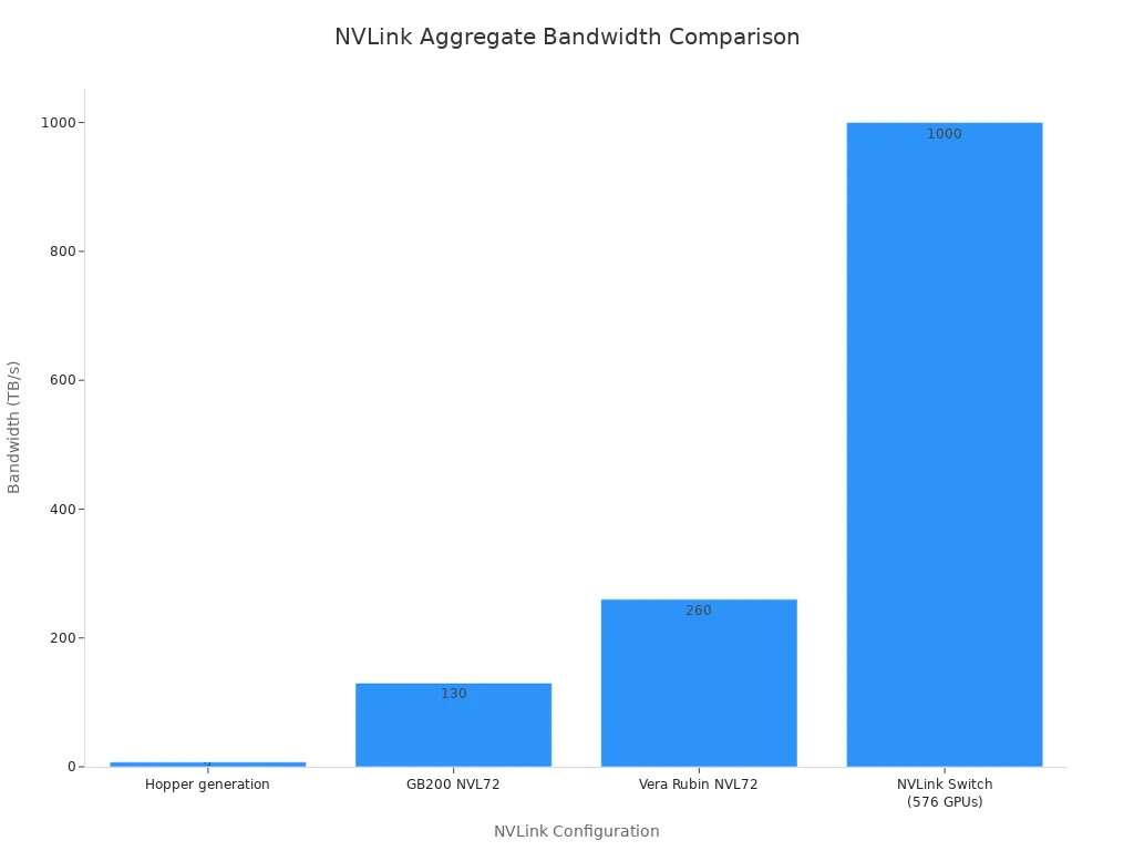
Rack-scale designs like NVIDIA Vera Rubin NVL72 link 72 GPUs in an all-to-all setup for a total of 260 TB/s, giving huge bandwidth for the all-to-all communications that training and inference of top mixture-of-experts model architectures need.
PCIe 5.0 links on accelerator cards carry 32 Gbit/s per lane in each direction. The real payload bit rate comes out near 31.5 Gbit/s. These speeds need controlled impedance in every part.
Power Density and Thermals
Current needs grow just as quickly. A GPU cluster pulls hundreds of amps through the PCB. Edge AI devices like NVIDIA Jetson squeeze the same current density into much smaller boards. AI server PCBs now range from 8 to 40 layers. GPU boards often go past 24 layers and cost more than $5,000 each.
You have to plan thermal management and high-current delivery together with signal routing. Copper weight, via count, and plane design all change how heat spreads. A trace that carries power also sends heat into nearby signal layers. High-performance computing boards fail when engineers treat power and signal as separate issues. Plan thermal management early, or you will have to re-spin the board.
Signal Integrity in High-Speed PCB Design
Impedance Control and Reflections
Every trace on your board has a characteristic impedance. This value comes from trace width, dielectric thickness, and the dielectric constant of your material. When impedance changes along a route, part of the signal bounces back to the source. That reflection harms the data eye and increases bit error rates.
You must keep impedance steady across the whole channel. A connector, a via, or a layer transition all cause impedance discontinuities. Each one adds reflection. In high-speed pcb work, even a small mismatch builds up across many links.
Fabricators build to a tolerance window for controlled impedance traces. According to MCLPCB, the standard final impedance tolerance sits near +/- 10%. QueenEMS confirms that many commercial PCB builds use this same +/- 10% window. Tighter tolerances raise cost sharply, and a fabricator may mark your request as an error.
Keep your impedance target inside the +/- 10% window unless your design risk truly demands tighter control.
This rule protects signal integrity without inflating your budget. You should also simulate your stackup before release. A field solver shows you where reflections will hurt the most.
Termination Strategies
Termination absorbs signal energy at the end of a trace. Without it, reflections bounce between the driver and receiver. You have several options, and each fits a different topology.
Series termination places a resistor near the driver. Parallel termination places a resistor to a reference voltage at the receiver. Both work well for point-to-point nets. For memory interfaces, the industry favors a different approach.
JEDEC DDR5 specifications require termination schemes to fight high-frequency effects like reflections and crosstalk. Intel's signal integrity methodology for DDR5 uses on-die termination, or ODT. Micron applies ODT circuits in DDR4 and DDR5 systems, along with write leveling and read training, to correct signal degradation at multi-gigabit speeds. ODT puts the resistor inside the chip. This placement shortens the stub and reduces parasitic effects.
You should match your termination choice to the interface. A high-speed serial link may need AC coupling plus parallel termination. A DDR5 bus relies on ODT and training algorithms. Get this wrong, and your eye diagram collapses at the receiver.
Simulate each net with the actual driver and receiver models. Then verify your termination values against the manufacturer's reference design. This step catches mistakes before you commit to fabrication.
Stackup and Material Selection
Your stackup design decides whether your high-speed signals make it through in one piece. Regular FR4 can't keep up with the speeds AI processors run at. At 10 GHz, FR4 has a dissipation factor of 0.02. You need low-loss dielectrics with Df values under 0.004.
Low-Loss Dielectrics and Copper Roughness
Low-loss materials in 16+ layer AI server PCBs show Dk between 3.0 and 3.5 and Df from 0.0017 to 0.004 at 10 GHz. FR4 has Dk of 4.2 and Df of 0.02, so it doesn't work for high-frequency designs. Megtron 7, Tachyon 100G, Astra MT77, and Rogers RO4350B keep impedance steady above 10 GHz. These materials work with PCIe Gen5, NVLink, and CXL.
Copper roughness changes signal loss just as much as the dielectric does. Dropping surface roughness from 3.0 μm to 1.5 μm cuts insertion loss by about 0.1 dB/inch at 10 GHz. That gain grows to 0.3 dB/inch at 50 GHz. Standard ED copper has a rough surface that raises loss at high frequency. Smooth copper foil lowers that loss a lot.
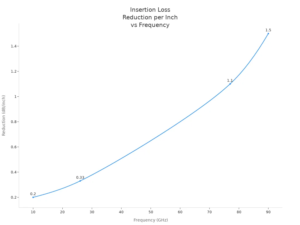
At 10 GHz, the gap between standard ED and smooth RA copper is 0.20 dB/inch. At 26 GHz, that gap widens to 0.33 dB/inch. On a 10-inch trace, the savings add up to several dB of channel margin. You can't give up that loss in an AI server.
Thermal management shapes which material you pick. AI processors give off 700W or more. The laminate has to survive those temperatures. Low-loss materials have higher glass transition temperatures than FR4, which helps them handle repeated thermal cycles.
Layer Count and Reference Planes
An NVIDIA H100 board needs 22 layers. Server boards for H100 or GB200 run from 20 to over 40 layers. They use ultra-low-loss laminates and HDI construction. They handle multi-terabit interconnects and power loads over 700W.
Each extra layer has a job. Signal layers carry data between processors and memory. Power planes spread current around. Ground planes give return paths. A high-speed pcb design with 22 layers includes signal, ground, power, and routing layers. Ground planes act as reference planes for stripline routing.
Reference planes control the impedance of every trace above them. Pair each signal layer with a ground plane right next to it. Without a steady reference, return currents take long paths and create loop inductance. This leads to ground bounce and weaker signals. Stitch ground planes together with vias near every layer transition. Plan your stack with symmetric construction so the board doesn't warp.
Routing Best Practices for High-Speed PCB
Differential Pairs and Length Matching
You use differential pairs on every high-speed link in an AI board. Each trace should have a characteristic impedance a little above 50 ohms. Keep both traces the same width so the differential impedance is exactly 100 ohms. This makes the odd-mode impedance about 50 ohms.
The exact width and spacing depend on your stackup. For 100-ohm differential impedance on a 1.6 mm FR-4 board, start with a trace width of about 5 mils and a spacing of about 8 mils. Check these values with an impedance calculator or field solver.
Dielectric thickness (mils) | Approx. trace width (mils) | Approx. spacing (mils) |
|---|---|---|
5 | ~6.2 | tight coupling, spacing varies with stackup |
45 | varies | larger spacing needed as thickness increases |
60 | varies | width-to-spacing ratio depends less on distance to ground |
Tight coupling is not strictly required for a differential pair to work correctly.
Glass-weave skew threatens timing alignment on high-speed, high-layer-count boards. Timing skew for an open weave can reach 4 ps/inch or higher on common glass weaves. That skew throws two fast signals out of sync. Angled routing at about 2.3 degrees cuts skew standard deviation from about 7 ps/in to under 1 ps/in.
In differential pairs, skew disrupts common-mode noise rejection and can significantly degrade eye diagrams, jitter margins, and bit-error rates.
Via Optimization and Stub Control
Via stubs create resonance that destroys signal integrity at high frequency. Aim for a via stub length under 15 mils (0.38 mm) to avoid resonance in the operating bandwidth. Above 10 GHz, keep via stubs under 5 mils.
Backdrilling removes the unused via stub from the back side of a through-hole via in high-frequency designs. Residual stub length is usually 5–15 mil. This range gives return loss of –15 to –20 dB at 28 GHz.
Quarter-wave resonance follows f = c / (4 × stub_length × √Dk), where c is the speed of light and Dk is the dielectric constant. For Rogers RO4350B (Dk=3.48), a 2 mm stub resonates at about 20 GHz. Backdrilling moves that resonance above the operating frequency for high-speed designs.
Power Integrity for AI Processors
Power integrity decides if your AI processor stays inside its core voltage range. You must build the PDN to send clean power at all frequencies. If this fails, you get random resets and damaged data.
Decoupling and Capacitor Placement
Decoupling capacitors are the base of your power integrity plan. Each package size covers a different frequency range. The table below shows the normal picks.
Package | Typical ESL | Typical Value Range | Best Application |
|---|---|---|---|
0805 | 0.5–1.0 nH | 1 µF to 10 µF | Bulk decoupling |
0402 | 0.3–0.5 nH | 10 nF to 100 nF | Local IC decoupling |
0201 | ~0.3 nH | 100 pF to 10 nF | High-speed, >100 MHz decoupling |
Put high-frequency caps right next to the power pin. The lowest-value capacitors must sit closest to the die. Every millimeter of trace adds inductance.
You pick X7R or X5R ceramics for power decoupling in your ai hardware. These materials hold capacitance well across temperature and DC bias voltage. Always check the DC bias derating curve for the capacitor you choose. A 0402 capacitor can lose 60–80 percent of its rated capacitance under rated voltage because of DC bias sensitivity. Y5V does even worse and should never be used.
A normal design pairs a 1 µF capacitor for lower-frequency fundamentals with smaller values like 100 nF, 10 nF, and 100 pF. These target the higher-order switching harmonics from the processor cores. You place the smallest capacitance values closest to the processor power pins. Use values from 0.01 µF to 0.1 µF for high-speed decoupling. Bigger capacitors like 10 µF or 100 µF handle low-frequency transients and steady the supply.
Place multiple identical capacitors in parallel. This stops resonance peaks and gives broadband performance. Every capacitor has a self-resonant frequency. By paralleling identical values, you spread the bandwidth and lower impedance.
Follow a simple placement rule. Use multiple decaps of the same value near the power supply. If not possible, add the lowest-value capacitor closest to the power supply. This cuts loop inductance and boosts your PDN performance. Place vias as close to the capacitor pads as possible.
PDN Impedance and Voltage Ripple
Your PDN must show a target impedance from DC to several hundred megahertz. You figure this target as the allowed voltage ripple divided by the maximum transient current. The PDN impedance must stay below this value at every frequency. A peak above the target causes voltage droop at the die.
Modern AI processors run at sub-1V core voltages with tight tolerances. A 3 percent tolerance on a 0.8V core gives you only 24 mV of room. Voltage ripple above this limit makes the processor malfunction. Your bulk capacitors handle low-frequency ripple below about 1 MHz. Mid-frequency decoupling from 0402 and 0805 capacitors covers 1 MHz to 100 MHz. High-frequency decoupling from 0201 capacitors and on-package capacitance handles frequencies above 100 MHz. You must cover all three ranges to keep steady voltage at the die.
You must simulate the full PDN impedance profile before layout sign-off. The simulation shows where impedance peaks cross your target. You adjust capacitor count, values, and placement until the profile fits within the target envelope. Without this step, voltage ripple can go past the specification and cause failures in your ai hardware. Use a SPICE simulator or a PDN analysis tool. Include the parasitic inductance of vias and planes in your model.
Power integrity is a system-level problem in advanced PCB design. The VRM has its own output impedance that interacts with the board impedance. The PCB planes add inductance and capacitance. The decoupling capacitors fill in the gaps where plane impedance rises. The on-chip capacitance handles the fastest transients. Optimize every element as a single system. Check your PDN simulation against measurements on the prototype.
EMI and EMC Mitigation for AI Hardware
Shielding, Filtering, and Grounding
Your AI server sends out energy from every high-speed trace and power plane. You have to stop that energy before it gets out of the chassis. Conductive foam gaskets are a strong first line of defense. The SOFT-SHIELD 4800, 4850, and 4860 models each reach 95 dB of shielding effectiveness from 20 MHz to 10 GHz. The 4840 model drops to 60 dB over the same range. Choose the higher-performing gaskets for slots and seams near your fastest links.
Filtering stops noise from getting out through cables. Put ferrite beads and common-mode chokes on every external interface. Ground the filter return to the chassis, not to signal ground. This keeps noise currents out of your signal reference.
Know your regulatory target before you design. FCC Part 15 Class B sets radiated emission limits for unintentional radiators at 3 meters.
Frequency range (MHz) | Radiated emission limit at 3 m (µV/m) |
|---|---|
30–88 | 100 |
88–216 | 150 |
216–960 | 210 |
Above 960 | 300 |
Class B applies to residential environments and is about 10 dB stricter than Class A. AI server equipment usually sits in data centers, so it typically falls under Class A. Confirm your classification with your marketing team early.
Ground Plane Stitching and Return Paths
Return currents follow the path of least impedance. At high-frequency, that path runs directly under the signal trace in the reference plane. Any gap in that plane forces the return current to take a detour. The detour creates a loop, and the loop radiates.
Stitch your ground planes with vias to close those gaps. Keep via stitching spacing below one-twentieth of a wavelength at your highest operating frequency. This rule stops the gap between vias from acting as a radiating antenna. At 20 GHz in FR-4, the wavelength is 7.5 mm, so your spacing must stay at or under 0.375 mm. At 10 GHz, the limit is 0.75 mm. For designs above 3 GHz, consider spacing at one-tenth of a wavelength or tighter.
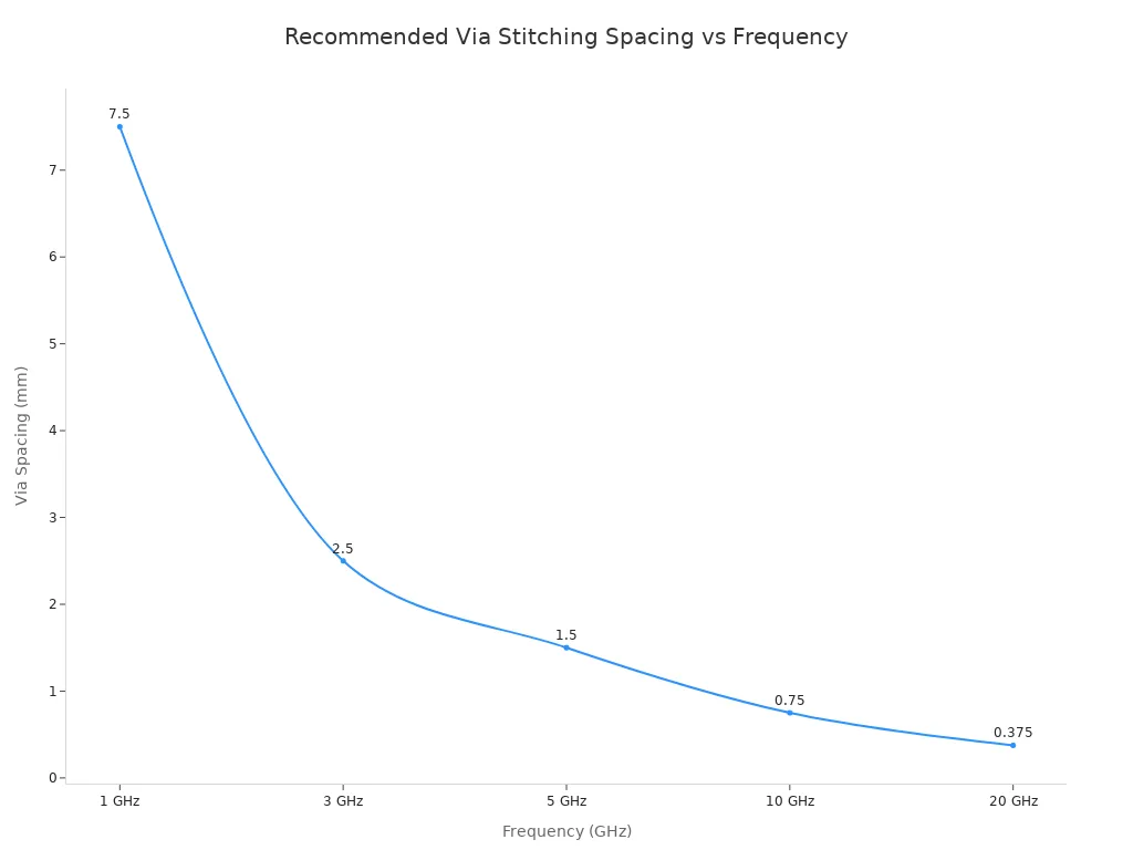
Place stitching vias near every layer transition and along board edges. This practice controls edge radiation and gives every signal a clean return path.
High-Speed PCBA Manufacturing and Testing
DFM Rules and Impedance Tolerance
Your high-speed pcba partner must keep tight tolerances on 16+ layer and HDI boards. Standard boards handle 5–6 mil traces. Advanced builds reach 3–4 mils. Specialty processes go below 3 mils and need special equipment and skills.
PCB Type | Minimum Trace Width / Spacing | Notes |
|---|---|---|
High-density designs | 4 mil / 4 mil | Typical sweet spot for most high-density PCBs |
High-end HDI applications | 2 mil / 2 mil | Reserved for advanced HDI processing |
Advanced HDI (laser drilling microvia) | 2 mil / 2 mil (0.05 mm / 0.05 mm) | Used in ultra-thin, high-density applications such as smartphones and RF modules; costs increase significantly |
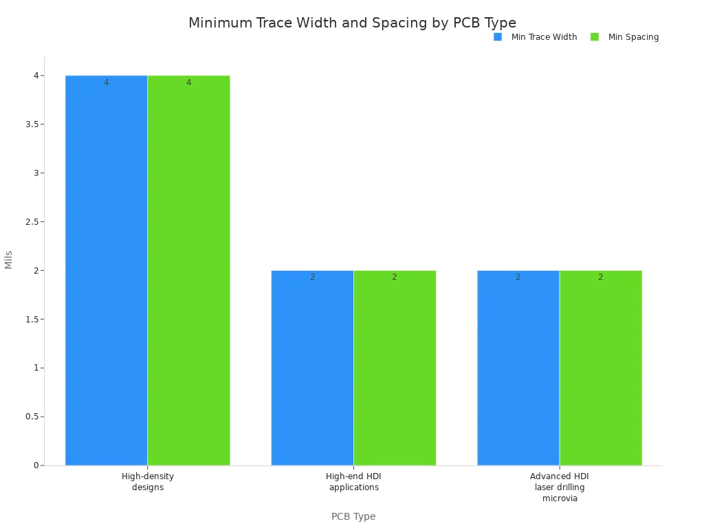
The push for even higher density is driving the development of ultra-fine line widths/spaces (25 μm and below) and microvias with diameters under 10 μm—enabled by advanced laser drilling and photolithography techniques.
Check DFM rules before you release artwork. Make sure your fabricator can hit your impedance target inside the +/- 10% window. Ask for a stackup review and a coupon design that matches your real traces.
Signal Loss Measurement and Validation
You must check every high-speed pcba build with test coupons. Coupons sit on the panel edge and carry the same trace shape as your design. Measure impedance on these coupons with a TDR. Compare the result against your target and the tolerance window.
Insertion loss comes next. Use a vector network analyzer on coupon traces. Check loss at your operating frequency and compare it to your simulation. A gap between measured and simulated loss points to a material or copper roughness problem.
Build a high-speed pcba validation flow into every order. Require impedance coupons, insertion-loss data, and a first-article report. This step catches drift before volume production. A high-frequency failure at this stage costs far less than a field return.
You now have a full design plan. Control impedance, choose low-loss materials, match differential pairs, improve vias, build the PDN, reduce EMI, and check everything with test coupons. Each rule guards signal integrity, power steadiness, or manufacturability. None of them are just pointless rules.
Before you approve your layout, run a stackup simulation. Then look over your fabricator's DFM rules. These two steps catch high-speed problems while they still cost nothing to fix. Your ai hardware needs that care.
FAQ
Why do AI PCBs need so many layers?
AI processors need a lot of bandwidth and power. More layers give you separate signal, ground, and power planes. These layers help control impedance and handle heat. A typical GPU board uses 22 layers or more.
What materials should you use for high-speed signals?
Use low-loss laminates like Megtron 7 or Tachyon 100G. They have a dissipation factor below 0.004 at 10 GHz. Regular FR4 has a Df of 0.02, which causes too much signal loss at high speed.
How do you prevent signal reflections?
Keep impedance steady along every trace. Use termination resistors or on-die termination. Match your stackup to the target impedance. Simulate each net before you send the design to fabrication.
When should you use backdrilling?
Use backdrilling when via stubs cause resonance above 10 GHz. Remove the unused stub to keep it under 5 mils. This improves return loss and avoids signal degradation.
How do you validate your design?
Use test coupons on your panel. Measure impedance with a TDR. Check insertion loss with a VNA. Compare results to your simulation. Always require a first-article report from your fabricator.
See Also
High-Speed PCB Design: Definition and Its Critical Role
Selecting Optimal Materials for High-Speed PCB Design Success
The Basics of High-Speed PCBs: Definition and Significance
Essential Knowledge for Mastering PCB Multi-Layer Circuit Board Layout
Key HDI PCB Manufacturing Considerations for Reliable Boards
