How to Maximize Signal Transmission Performance in High Speed PCB Designs

You want your high-speed pcb to work well and send signals reliably. First, know that signal integrity is very important in high-speed pcb design. Things like impedance mismatches and crosstalk can hurt signal quality. This can cause errors and more failures. When you plan pcb design, think about material choice, trace layout, and noise reduction. If you use these ideas early, you help performance and lower the chance of problems. Look at your current process to find ways to make it better and keep signal quality strong.
Key Takeaways
Pick materials with low dielectric constant (Dk) and low dissipation factor (Df) for high-speed PCBs. This helps signals stay clear and lowers signal loss.
Keep trace width and spacing the same to control impedance. Doing this stops signals from bouncing back and makes performance better.
Use differential pair routing for important signals. This makes sure both paths are the same length, so there are fewer timing mistakes and signals stay strong.
Use the right termination methods to stop signals from bouncing back. Make sure resistor values match the trace impedance to keep signals good.
Check impedance carefully with simulation tools. Finding problems early helps your PCB design work well.
High-Speed PCB Material Selection
Dielectric Properties and Signal Integrity
The material inside your pcb can change how signals move. The dielectric constant (Dk) tells you how fast signals go through the board. If Dk is lower, signals move faster and stay strong. The dissipation factor (Df) shows how much energy turns into heat. If Df is high, you lose more signal strength. This makes your transmission weaker. For high-speed designs, you want Dk and Df to be low. This keeps signals clear and stops problems like signal loss and distortion.
Tip: If Dk and Df are low, your signal quality stays high. This helps your pcb work better, especially with high-speed designs.
Comparing Materials for High-Speed Designs
You can pick from many pcb materials. Each material has different features that change how your board works. Here is a table that shows common materials:
Material | Dielectric Constant (Dk) (@ Frequency) | Typical Applications |
|---|---|---|
FR-4 (Glass Epoxy) | ~4.2 (1-10 MHz), ~4.0 (1 GHz) | General-purpose PCBs, low-cost electronics |
High-Speed Epoxy | 3.5-4.0 (stable) | High-speed digital (computers, networking) |
Polyimide (PI) | ~3.5-4.0 | Flexible PCBs, high-temperature applications |
PTFE (Teflon) | ~2.2-2.5 | RF/microwave circuits, high-frequency apps |
Rogers RO4350B | 3.48 (10 GHz) | RF/microwave, high-frequency digital |
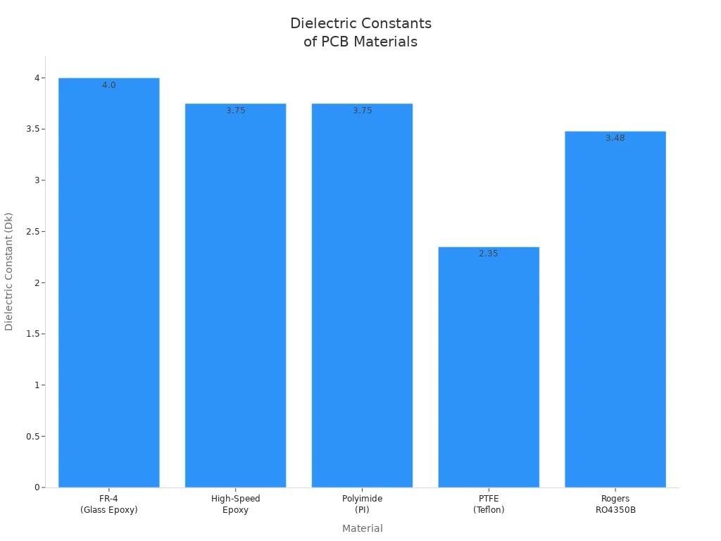
FR-4 is cheap, but it loses more signal at high frequencies. Rogers materials lose less signal and keep quality better. They can show up to 35% less signal loss than FR-4. This makes Rogers a great choice for high-speed designs that need strong performance.
Practical Selection Tips
When you choose a pcb material, do not just look at price. You should check these important things:
Dielectric constant (Dk): Lower Dk helps signals move faster and controls impedance.
Loss tangent (Df): Lower Df means less signal loss and better performance.
Glass transition temperature (Tg): High Tg makes your board more reliable when it gets hot.
Thermal conductivity: Good heat flow stops your board from overheating.
Coefficient of thermal expansion (CTE): Matching CTE with parts stops cracks or failures.
FR-4 costs less, about $0.50 to $1.50 for each square inch. Rogers and other advanced materials can cost $5 or more for each square inch. For designs above 5 Gbps, pick materials with low Dk and Df, even if they cost more. This keeps your signal strong and your board working well.
Trace Routing Optimization in High-Speed PCB Design
Trace Width and Spacing for Performance
You can make your pcb work better by picking the right trace width and spacing. Wider traces have less resistance. This keeps signals strong. Always use the same width and spacing for traces. This helps keep impedance correct and stops signal reflections. Single-ended signals should have 50 ohms impedance. Differential pairs should have 100 ohms impedance. The space between traces is very important. If traces are too far apart, impedance goes up and signal quality gets worse. For example, spacing of 8 mils on FR-4 keeps impedance close to 100 ohms. If you change it to 12 mils, impedance can go up to 110 ohms. This can make performance drop. Keep traces at least three times their width apart. This lowers crosstalk and noise.
Differential Pair Routing in High-Speed Designs
Differential pair routing is very important for high-speed systems. Both traces in a pair must be the same length. This stops timing errors and keeps signals strong. Route pairs side by side with smooth corners. This keeps their paths equal and helps performance. Use length-tuning if you need to match paths. Keep differential pairs away from single-ended signals. This stops crosstalk. Only use vias when you must. Too many vias can weaken signals and lower quality. Balanced routing helps lower ground bounce and keeps the system working well.
Return Path Management
A clear return path is needed for high-speed designs. If the return path is broken, signals can wander. This makes electromagnetic interference. Signal quality gets worse and transmission is hurt. Fast signals need a smooth return path to stop distortion. Keep related signals on the same layer. Use as few vias as possible. This keeps the return path short and direct. Good return path management lowers crosstalk and noise. This makes performance better.
Impedance Control and Signal Integrity
Controlled Impedance Techniques
You need to control impedance in your pcb. This keeps signal quality high. If impedance does not match, signals can bounce back. This causes errors and hurts signal integrity. It also lowers how well your system works. You can use different materials and stackups to help control impedance. Look at the table below to see how materials affect transmission and signal attenuation:
Material | Dk (typical @10 GHz) | Df (typical @10 GHz) | Recommended Frequency Range | Key Advantages |
|---|---|---|---|---|
FR-4 | ~4.4 | ~0.020 | <5 GHz | Low cost, easy processing |
Rogers RO4003C | 3.38–3.55 | 0.0027 | Up to 20+ GHz | Stable Dk, easy to process |
Rogers RO4350B | 3.48–3.66 | 0.0037 | Up to 20+ GHz | Good thermal stability |
PTFE-based | 2.1–3.0 | <0.0015 | mmWave (5G/6G) | Ultra-low loss |
You can use tight trace width and dielectric control. This keeps impedance within industry standards. Most high-speed pcb designs need impedance tolerance of plus or minus 10 percent. Some applications, like PCIe Gen5 or RF, need tighter control of plus or minus 5 percent. If you keep trace width and dielectric thickness within 0.5 mil, you help maintain signal integrity.
Tip: Use materials with stable Dk and low Df for high-frequency transmission. This helps reduce signal attenuation and keeps performance strong.
Termination Methods for High-Speed Designs
Termination stops signal reflections. It keeps signal quality high. You can use two main methods. Series termination and parallel termination.
Series termination puts a resistor in series with the driver. Place it close to the source. This matches the driver’s impedance with the trace. It absorbs reflections.
Parallel termination puts a resistor in parallel with the receiver. This reduces reflections at the load end. You must place it carefully to avoid extra power use.
If you use proper termination, you improve signal integrity. Your eye diagram gets clearer. This helps your pcb work better and boosts system performance.
Note: Always match the resistor value to the trace impedance. This keeps signal integrity strong and lowers signal loss.
Impedance Verification Tools
You must check impedance to make sure your pcb meets design goals. You can use simulation and measurement tools for signal integrity analysis.
Tool/Technique | Description |
|---|---|
Altium’s Layer Stack | Lets you input dielectric constants and trace sizes to check controlled impedance at high frequencies |
Cadence Allegro | Offers advanced simulation for signal integrity analysis and crosstalk detection |
ANSYS SIwave | Gives detailed 3D electromagnetic field analysis for high-speed pcb designs |
HyperLynx | Provides signal integrity simulation and easy wizards for impedance-controlled traces |
TDR Simulation | Measures impedance discontinuities by analyzing reflected signals |
Pre-layout Simulation | Checks impedance before layout, lets you adjust design parameters |
Post-layout Simulation | Verifies actual design matches intended impedance after manufacturing |
You can also use hardware tools like time-domain reflectometry (TDR) and vector network analyzers (VNA). TDR finds impedance changes along the transmission line. VNA shows signal loss in the frequency domain. These tools help you spot problems and improve signal integrity.
Tip: Use signal integrity simulation before and after layout. This helps you find issues early and keeps signal quality high.
If you follow these steps, you keep impedance under control. You boost performance in your high-speed pcb. You protect signal integrity and make sure your transmission stays strong.
Noise Reduction and Crosstalk Minimization
Grounding Strategies for Performance
You can make high-speed pcb designs work better with good grounding. Multi-point grounding helps stop EMI and keeps signals clear. Try to keep ground loop areas small to cut down on noise. A good grounding plan lowers crosstalk and noise. It also keeps signals strong and protects your board from EMI. Solid ground planes let return currents move easily. This keeps electromagnetic interference low and stops timing mistakes. Always give high-speed signals a steady reference plane for their return path. Never split ground planes. This can cause ground loops and more noise.
Tip: Put decoupling capacitors close to power pins. This filters noise and keeps the power supply steady.
Shielding and Isolation in High-Speed PCB
Shielding and isolation are important in high-speed pcb designs. How well shielding works depends on coverage, material, and frequency. Foil shields block high-frequency noise almost all the way. Braided shields are good for low-frequency noise and are flexible. You need to think about cost and weight when you pick shields. Guard traces can lower crosstalk by up to 20 dB in crowded layouts. Put guard traces on both sides of important high-speed traces. This is needed for clock or data lines above 500 MHz. Connect guard traces to the ground plane at many points with vias. Make guard traces as wide as the signal trace. Keep a space three times the trace width between them. Always route differential pairs close together with even spacing. Use ground planes and shielding to keep sensitive signals away from noisy spots.
Keep enough space between signal traces.
Route high-speed signals on different layers with ground planes in between.
Do not run long traces side by side.
EMI and Reflection Reduction
You can lower EMI and reflections by using some simple steps. High-speed signals above 50 MHz can act like antennas and send out EMI. Switching circuits and long cables also make noise. Bad pcb layout, like big loop areas or traces too close, makes things worse. Use short traces and solid ground planes to cut down EMI. The table below shows ways to fight EMI and reflections:
Strategy Type | Description |
|---|---|
Shielding Techniques | Grounded shields and enclosures block EMI and improve attenuation. |
Grounding Strategies | Solid ground planes reduce inductance and stabilize the pcb. |
Signal Filtering | Capacitors and ferrite beads absorb and block unwanted EMI. |
Use simulation tools to find impedance mismatches and reflections. Make sure termination resistors match the trace impedance. Check vias and connectors for problems and use as few as you can. These steps help keep signal quality high and make data transmission reliable in high-speed systems. Good noise control makes your system work better and lowers signal loss.
Connectors and Vias in High-Speed PCB Design
High-Speed Connector Selection
You must pick connectors carefully for high-speed pcb designs. Connectors are important for sending signals and keeping them clear. If you send data faster than 10 Gbps, you should think about these things:
The connector should have matched impedance for your bandwidth.
Low insertion loss keeps signals strong.
The connector must connect well to the pcb and cables.
S-parameters show how much signal is lost and what bandwidth the connector supports. They help you know if the connector works well for high-speed systems.
There are different connector types you can use:
Surface mount connectors are flexible and good for high-speed designs.
Press-fit connectors are strong but might not work well at high speeds.
Paste-in-hole connectors have short pins and can work better at high frequencies.
Always check the connector’s specs to see if it fits your design.
Via Design for Signal Integrity
Vias link layers in your pcb. They are important for signal quality and how well signals move. You need to look at via shape and size. A high aspect ratio means the board is thick compared to the hole. This can lower resistance and help match impedance. If the aspect ratio is too high, stubs can form and hurt signal quality. Back-drilling cuts off extra via length and stops this problem.
Vias are very important for high-frequency pcb designs.
Small changes in via shape can cause reflections and crosstalk.
Good via design keeps signals clear and lowers bit errors.
Keep vias short and use back-drilling if needed. This helps keep signals strong.
Minimizing Parasitic Effects
Parasitic capacitance and inductance can make signals worse in high-speed pcb designs. You can lower these effects by doing a few things:
Do not route traces in parallel and keep them short.
Use fewer vias and keep high-speed signals on the same layer.
Pick dielectric materials with low permittivity.
Use shielding like guard rings or Faraday shields.
Make sure there is a solid ground plane under signal traces. Do not split the ground plane.
These steps help keep signals strong and clear in your pcb. If you manage connectors and vias well, your high-speed data will move reliably in your system.
You can make your high-speed pcb work its best by using smart steps. Pick materials that do not lose much signal. Keep traces as short as you can. Make sure impedance matches to keep signals safe. Use differential pair routing and solid ground planes to cut down noise. New materials and simulation tools help you fix problems before you build your pcb. Always learn about new ways and check your designs often. This helps your high-speed pcb stay strong and reliable.
FAQ
What is simulation in high-speed PCB design?
Simulation lets you check your PCB before building it. You can see how signals move on the board. This helps you find problems early. You can fix issues before making the PCB. Simulation can test different parts of your board.
Why do you need analysis for signal transmission?
Analysis helps you see how signals travel in your PCB. You use it to find mistakes and make your design better. Analysis checks things like impedance, noise, and signal quality. It gives you facts to help your PCB work well.
How do simulations help with signal integrity?
Simulations show how signals act in your PCB. You can check for crosstalk, reflections, and noise. Simulations let you try out different layouts and materials. You can see if your design keeps signals strong.
Can simulation and analysis prevent signal quality issues?
Simulation and analysis help you find problems before building your PCB. Simulation lets you test changes to your design. Analysis shows what works best. Using both makes your PCB reliable and fast.
What tools do you use for simulation and analysis?
You can use tools like Altium, Cadence, and ANSYS. These tools let you run simulations and check your design. You can use them to look at impedance, noise, and signal strength. Simulations help you make good choices.
See Also
Top Materials for Designing High-Speed Printed Circuit Boards
Understanding High-Speed Printed Circuit Boards and Their Uses
The Importance of High-Speed PCB Design Explained Clearly
