Multi-layer High TG PCB Stack-up Design

Your multilayer PCB stackup must survive harsh conditions. Industrial electronics often work from -40°C to 170°C. Normal materials fail at these temperatures. A high TG PCB stack-up keeps its structure and electrical performance. You need this reliability for automotive, aerospace, and high-power uses.
Your PCB stack-up design faces competing needs. Thermal stability requires strong materials. Signal integrity demands controlled impedance. Your stack-up must balance these needs. High-speed signals need exact dielectric spacing. High-frequency circuits suffer from material losses. A good stack-up handles both heat and signal quality.
Think about your circuit board design carefully. Each multilayer layer affects impedance and heat behavior. Plan your stackup for signal quality and mechanical strength. A proper PCB stack-up stops delamination and warpage. Your circuit board works well when you match materials to needs. Controlled impedance traces and a balanced stackup design lead to success. This PCB stack-up protects your signal paths. Your whole stack-up strategy decides final performance.
Key Takeaways
High Tg materials help keep PCB layers stable in extreme heat or cold.
Balance heat resistance with signal quality for the best results.
To stop warping and cracks, use a symmetrical stack-up.
Select materials such as high Tg FR-4 or polyimide for your needs.
Talk to your manufacturer early to manage signal flow and prevent mistakes.
High TG PCB Stack-up: Core Design Factors
Thermal vs. Signal Integrity Trade-offs
Picking a high Tg material often clashes with what you need for performance. A higher glass transition temperature can lead to a higher dielectric constant. This shift directly impacts your signal paths. You have to find a balance between thermal stability and signal quality.
How are material properties different? Standard FR-4 has a dielectric constant around 4.2-4.8 at 1 MHz. High-Tg FR-4 with a Tg of 170°C shows a Dk of 4.0-4.5 at the same frequency. High-Tg FR-4 at 180°C drops further to 3.8-4.3. The pattern repeats at 1 GHz. The table below shows these values clearly.
Material | Dielectric Constant @ 1 GHz |
|---|---|
Standard FR4 | ~4.2 - 4.7 |
High Tg FR4 | ~4.2 - 4.6 |
High Tg material does not automatically ruin your signal. The values overlap a lot.
The dissipation factor matters more for high-frequency work. Standard FR4 has a Df of about 0.02 at 1 GHz. This causes too much signal loss above 1 GHz. High Tg laminates can reach a low dissipation factor. Materials like Panasonic R-1755V offer better performance. A lower Df cuts signal loss at high frequencies. This keeps your signal intact during operation.
You also need to match your material to your design needs. For lead-free soldering, experts suggest 170-180°C for larger parts. Standard thickness boards of 1.6mm need at least 170°C. This temperature ensures your multilayer pcb stackup survives the reflow cycle.
To balance these trade-offs, change your dielectric thickness. Thicker prepreg between your signal layer and the nearby plane helps control impedance. You can also pick materials with a low dissipation factor. This way keeps signal quality while meeting thermal needs. Your high tg pcb stack-up must serve both needs equally. A careful multilayer design handles all these factors.
Mechanical Robustness and Layer Symmetry
Mechanical strength depends on CTE values. The coefficient of thermal expansion differs between materials in your board. The table below shows the key values.
Material | Z-axis CTE (ppm/°C) |
|---|---|
Copper | 17 |
High-Tg FR4 (below Tg) | 40–50 |
High-Tg FR4 (above Tg) | 180–220 |
Copper expands at 17 ppm/°C. High-Tg FR4 below its Tg expands at 40-50 ppm/°C. Above Tg, this jumps to 180-220 ppm/°C. This mismatch creates mechanical stress on plated through-holes during thermal cycling. Repeated cycles cause fatigue and lead to barrel cracks. High Tg materials reduce the mismatch compared to standard FR4 but do not remove it.
Your pcb stack-up must be symmetrical to stop warpage. During reflow, the PCB temperature rises to 230-250°C. The resin softens and materials expand. Uneven copper distribution causes unbalanced thermal expansion. A layer with 90-95% copper paired with a layer at 20-40% copper creates bending stress. A full ground plane on one side with scattered traces on the other side bends the board. Dielectric thickness imbalance also causes issues. Thicker resin layers shrink more during curing. Your pcb stack-up needs careful planning to avoid these problems.
During reflow, an asymmetrical stack-up creates uneven thermal expansion. The CTE mismatch becomes more obvious. Internal stress spreads unevenly, leading to board deformation. A symmetrical stack-up design stops this problem. Use a balanced pcb stack-up in your design.
Your stackup design should mirror layer construction from the center outward. Use the same copper weight and pattern density on each side. This symmetry lowers internal stress and stops board deformation during soldering. A balanced stackup ensures compatibility between thermal and mechanical needs. Proper stackup design looks at both thermal and electrical factors. Your power delivery network and ground planes must balance across the stack-up.
A well-planned stack-up improves electromagnetic compatibility. Nearby power and ground planes provide return paths for high-speed signals. This setup reduces EMI and keeps controlled impedance for your signal layers. Controlled impedance traces rely on steady dielectric spacing and copper geometry. Your multilayer circuit board gains from this careful setup. This stack-up supports your high-speed design needs.
Power integrity also depends on your stack-up choices. The power delivery network needs low-impedance paths between power and ground. Thin dielectric layers between planes create capacitance. This capacitance supports current demands. Your stackup must balance all these needs.
Signal integrity and power delivery both start with the stack-up. High-speed signals need clean return paths and steady impedance. Your design must account for every layer and every material choice. A sound stackup stops manufacturing defects. Your overall stack-up strategy decides final performance.
Multilayer PCB Stackup: Layer Sequencing and Materials
Your layer order controls how your board handles noise and heat. A smart multilayer pcb stackup puts planes in the right spots. Every signal layer needs a nearby reference plane. This setup creates clean return paths. It also stops electromagnetic compatibility issues before they start.
Arranging Signal, Power, and Ground Planes
Begin with your ground planes. They support every signal return path. Put a solid ground plane right below each high-speed signal layer. This rule always applies. A power plane can work as a reference, but ground is better. Pick ground whenever you can.
Layer Count | Recommended Stackup (Top to Bottom) | Key EMI-Reduction Feature |
|---|---|---|
4-layer | Signal (low-speed) – Ground – Power – Signal (low-speed) | Ground/power planes give reference for outer layers; avoid high-speed on outer layers |
6-layer | Signal (low-speed) – Ground – Signal (high-speed) – Signal (high-speed) – Power – Signal (low-speed) | High-speed signals sit on inner layers with nearby reference planes |
8-layer | Signal (low-speed) – Ground – Signal (high-speed) – Power – Ground – Signal (high-speed) – Power – Signal (low-speed) | Multiple ground/power planes give strong shielding for high-speed layers |
If you can pick between a power plane or ground plane as the nearby layer that gives a return path or signal reference, always pick the PCB ground plane.
A transmission line has a signal trace and its return path. In a stripline setup, ground planes above and below the trace keep the electromagnetic field inside the dielectric. Smaller dielectric spacing and a solid ground plane improve impedance control and field containment. This setup lowers radiated emissions. A solid ground plane can reduce emissions by up to 20 dB. Keep signal-to-reference spacing at 3–5 mils for high-speed signals. This tight spacing shrinks loop area and cuts noise.
Your pcb stack-up must also handle power integrity. Place power and ground planes next to each other on inner layers. Thin dielectric between them creates useful capacitance. This capacitance supports sudden current needs. Your stackup design should pair each signal layer with a reference plane. This pairing keeps signal integrity across your whole circuit board.
Selecting High Tg Laminates, Prepregs, and Copper Foils
Material choice drives your stack-up performance. Prepreg flows during lamination. It bonds layers together. Its thickness and dielectric constant directly control impedance. A small change in prepreg thickness shifts your target impedance noticeably. For example, raising prepreg thickness from 5 mils to 10 mils can drop impedance from roughly 50Ω to 45Ω on a microstrip. Stripline setups show similar sensitivity. Changes affect both sides of the trace. A 2Ω shift can distort signals at frequencies above 5 GHz.
High Tg laminates come in several grades. Compare your options carefully.
Attribute | High-Tg FR-4 (Tg170-180) | Polyimide |
|---|---|---|
Glass Transition Temp (Tg) | 170-180°C | 180-220°C |
Relative Cost | Cost-effective | More expensive |
Thermal Resilience | Suitable for lead-free soldering | Excellent high-temperature stability |
Flexibility | Rigid, limited | Flexible, suitable for rigid-flex |
Processing | Standard manufacturing compatible | Requires specialized processing |
Moisture Absorption | Lower | Higher |
Best Application | Automotive, industrial, high-power LEDs, high-density designs | Aerospace, defense, high-power electronics |
High-Tg FR-4 at 170–180°C fits most automotive and industrial needs. It handles lead-free reflow profiles with peak temperatures near 260°C. It also supports boards with more than six layers or thicknesses above 0.062 inches. Polyimide costs more but handles extreme environments. It also absorbs more moisture, so it needs pre-baking before assembly.
Copper foil choice affects high-frequency loss. Standard electrodeposited (ED) copper has a rough surface. Rolled annealed (RA) copper is much smoother. The skin effect explains why this matters. At high frequencies, current moves near the conductor surface. Skin depth decreases with frequency, making surface roughness more significant.
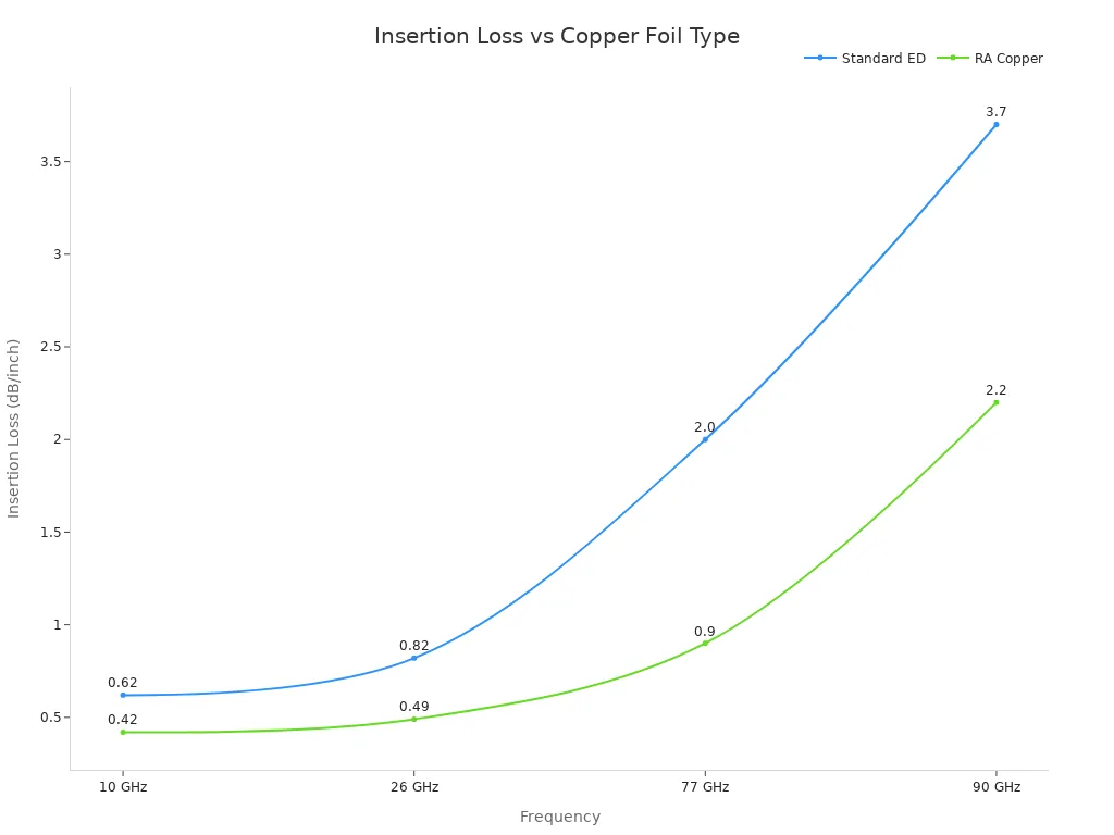
Standard ED copper has a rougher surface than RA copper. At high frequencies, RA copper exhibits lower insertion loss, making it preferable for designs above 10 GHz. Specify RA or smooth HVLP copper. Your high tg pcb stack-up will perform better with this choice. Match copper type to your frequency needs. This decision affects your controlled impedance traces directly. Your multilayer pcb stackup needs this attention to detail for best performance.
Impedance Control and Manufacturing Feasibility
Calculating Trace Width and Dielectric Thickness
Your impedance target starts with dielectric thickness. The space between your signal layer and its reference plane controls your final value. A smaller gap lowers impedance. A larger gap raises it. Use field solvers or IPC-2141 formulas to calculate trace width. These tools account for dielectric constant, copper height, and prepreg thickness. Your signal quality depends on this calculation.
Prepreg thickness carries a tolerance. Manufacturers specify ±10% for standard FR-4. This variation affects your controlled impedance.
A 10% variation in a 4-mil prepreg layer can shift impedance by 2-3 ohms, causing signal mismatches. For high-precision RF or high-speed digital designs, specify prepreg with ±5% tolerance.
Your stackup design must account for this shift. Use nominal thickness for initial calculations. Check your impedance at both tolerance ends. This check ensures your signal stays within requirements. Plan your multilayer stack-up with these tolerances in mind. Your pcb stack-up performance depends on meeting these requirements across manufacturing variations.
Navigating Drilling, Lamination, and Etch Constraints
Manufacturing limits affect your high TG stack-up. The drill aspect ratio limits via depth. High TG materials need careful lamination profiles. Your stack-up must survive these processes.
The etch process creates a trapezoidal trace shape. The etch factor describes this undercut. Several effects matter:
A lower etch factor produces a narrower trace. This profile increases characteristic impedance.
For differential pairs, undercut reduces trace width and increases the gap. This dual effect causes larger impedance changes.
Poor etch control leads to impedance mismatches, signal reflections, and degraded eye diagrams in high-speed links.
Your high-frequency routing needs tight etch control. Contact your fabricator early. Your high-speed traces depend on consistent geometry. Work with your manufacturer to set achievable tolerances for your pcb stack-up. This collaboration ensures your controlled impedance traces meet your needs. Your circuit board benefits from this approach. A good stackup accounts for manufacturing realities. Your multilayer design works reliably when you plan for real-world limits.
Example High TG PCB Stack-up Configurations
You need real examples to use these ideas. This part shows three common setups. Each one solves different problems. Use these examples as a starting point for your own multilayer pcb stackup design.
4-Layer and 6-Layer Stack-up Examples
A 4-layer pcb stack-up is a simple place to begin. Put routing layers on the outer layers. Place a ground plane on layer 2 and a power plane on layer 3. This setup gives each outer layer a close reference plane. Use high Tg FR-4 with a Tg of 170°C. This material can handle lead-free reflow profiles. Set your total board thickness to 1.6mm. This multilayer design works for low-speed designs and moderate heat needs.
A 6-layer pcb stack-up adds more ability. You get an extra ground plane and a second pair for routing. This multilayer design supports faster operation. The main benefit is having a dedicated ground plane next to every routing layer.
The key design idea behind this stack is to make sure every trace and power plane has a close reference plane, ideally a solid ground, to keep a low-impedance return path. This matters not just for high-speed uses, but for steady performance and less EMI in general.
The extra ground plane gives several benefits:
Low-impedance return paths: Every routing layer has its own ground plane right next to it, which lowers loop inductance and signal distortion.
Controlled impedance: Being close to a solid ground plane helps keep trace impedance steady, which reduces reflections.
Reduced EMI: Solid ground planes act as shields, blocking electromagnetic interference and stopping crosstalk between layers.
Stable power distribution: Multiple ground planes lower ground impedance, which improves power integrity and decoupling performance.
Support for high-speed traces: Designs like DDR4 memory need at least six layers to get these benefits, while a four-layer board lacks enough ground planes for all routing layers.
A typical 6-layer stackup puts routing layers on layers 1, 3, 4, and 6. Ground planes sit on layers 2 and 5. The power plane can share layer 5 if you split the plane. This layout keeps your paths short and your return paths clean.
8-Layer Stack-up with Mixed Signal Planes
An 8-layer pcb stack-up handles mixed-signal designs. You need to separate analog and digital sections. Multiple ground planes provide this separation. A typical setup uses four ground planes and two power planes. This gives you four routing layers.
Your stackup must be perfectly balanced from the center line. This includes copper weight, dielectric thickness, and material types. Balance stops the board from warping during high-temperature reflow soldering, which ensures high SMT production yields. A balanced 8-layer reduces warpage after reflow. This stackup configuration works well for complex designs.
Here is a practical 8-layer pcb stack-up. It uses a balanced construction with alternating prepreg and core layers. Signal layers use lighter copper, while ground and power planes use heavier copper. The prepreg thicknesses are chosen to achieve controlled impedance and a balanced stackup. The center core is thicker to provide mechanical stability. This stack-up mirrors the copper distribution from the center outward.
To reduce warpage, avoid uneven material stacks. Balance copper weights and copper density across layers. For mixed signals, place analog parts on layers 1 and 3. Place digital parts on layers 6 and 8. Ground planes on layers 2, 4, 5, and 7 separate these sections. This separation stops digital noise from leaking into analog paths.
Your high tg pcb stack-up needs this careful planning. You must meet impedance requirements for controlled impedance traces. Each setup has trade-offs for your pcb stack-up. Match the layer count to your complexity and heat needs. A well-planned stackup design gives you steady performance across temperature extremes. Think about your signal integrity needs when picking your stackup. The multilayer build of your circuit board directly affects impedance and high-frequency behavior.
Define your thermal and electrical requirements first. Choose appropriate high Tg materials. Sequence layers symmetrically. Validate controlled impedance with your manufacturer. These steps form your complete high tg pcb stack-up strategy.
Ignoring CTE mismatch between copper and laminate remains the most common pitfall. It causes via cracking or pad lifting. A successful multilayer pcb stackup requires collaboration between you and your fabricator.
Early manufacturer input optimizes layer count, avoids expensive processes, and improves yield. This partnership protects signal integrity and ensures reliability. Your stackup design must balance thermal demands with electrical performance.
Electric vehicles push operating temperatures higher. Mastering this multilayer stack-up becomes necessary. Apply these principles to your next circuit board project. Your pcb stack-up determines final performance.
FAQ
What Tg rating do I need for lead-free soldering?
For standard 1.6mm boards, pick a material with a Tg of at least 170°C. This rating can handle the 260°C peak reflow temperature. Your pcb stack-up must survive this heat cycle without separating layers. Boards with more layers may need Tg180 materials. Your stack-up design should match the heat needs of your assembly process.
How many layers should my multilayer design use?
Your layer count depends on how dense your routing is and what your signals need. A 4-layer stack-up works fine for simple designs. A 6-layer stack-up gives you solid ground planes next to every routing layer. An 8-layer stack-up keeps analog and digital sections apart. Match your stackup to your design's complexity. Each extra pair of layers boosts signal integrity and power delivery. Your signal quality gets better with each reference plane you add.
How do I control impedance in a high Tg stack-up?
Your controlled impedance depends on the dielectric thickness between the signal layer and its reference plane. Use a field solver to do the math. Keep in mind that prepreg thickness tolerances can move impedance by 2-3 ohms. For high-speed designs, ask for ±5% tolerance prepreg. Your stack-up needs this level of precision. A proper stackup keeps impedance stable even when manufacturing varies. Your signal paths stay clean when you manage this factor.
When should I consult my fabricator?
Talk to your fabricator before you lock in your stackup. They know their drill aspect ratios, etch factors, and lamination limits. Getting their input early prevents expensive changes later. Your multilayer pcb stack-up works better when you check your choices with them. This teamwork protects your circuit board. Your stack-up must also meet mechanical needs to prevent warping. A balanced stackup makes sure your final results match what you planned.
Can I mix standard FR-4 with high Tg materials?
You can mix materials in one stack-up, but be careful. Different CTE values create stress where layers meet. Your stack-up should stick with one material system throughout. Mixing prepreg and core from different suppliers can cause warping. A uniform stack-up gives you predictable results. Your signal integrity depends on consistent dielectric properties across every layer. This consistency matters for your high-speed signal paths.
See Also
Common HDI Multilayer PCB Stackup Configurations Explained
Challenges in Manufacturing and Prototyping Multilayer Circuit Boards
Evaluating Costs and Benefits of Stacked and Staggered Microvias in HDI PCBs
