PCB Thermal Stress Relief Techniques for Multilayer Boards
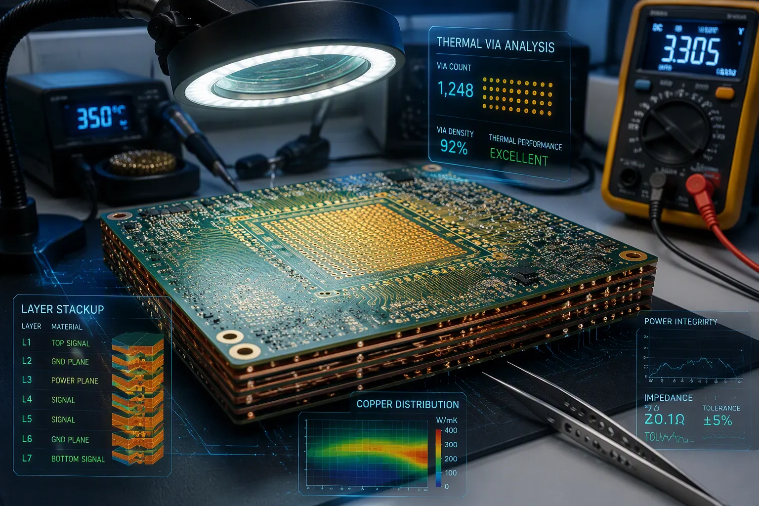
You fear four failure modes in multilayer PCBs: barrel cracks, pad lift, delamination, and warping. Each one starts with heat that the board cannot spread or absorb. PCB thermal stress relief is not a single fix. It is a discipline that spans design, material selection, and manufacturing. A printed circuit board with eight layers traps more thermal energy than a two-layer board. That trapped energy drives stress at every via and pad. You need a plan for temperature control at each stage. A thick copper plane pulls warmth away from a hot component. A thin trace cannot do that job. The same logic applies to every layer in the stackup. These steps protect reliability.
Key Takeaways
Put thermal vias under hot parts to carry heat away and lower stress.
Keep the copper even on every layer to stop warping and delamination.
Pick materials with matching CTE and high Tg to handle heat better.
Put heat-sensitive parts away from hot spots so they do not get damaged.
Check boards with heat stress tests to make sure they work well.
PCB Thermal Stress Relief Fundamentals
Why Multilayer PCBs Are Vulnerable
You do thermal stress analysis on multilayer PCBs to get thermal reliability, strong boards, and long-lasting durability. More layers and tighter routing pack in heat. They also make the CTE mismatch worse between laminate, copper, and components.
Several things make multilayer boards more open to thermal stress than single or double-layer boards:
CTE mismatch: More material boundaries mean copper and laminate expand at different rates, which builds up stress.
Via aspect ratio: Deeper vias often have a higher aspect ratio, so the copper plating is thinner. This thin coating cracks more easily under thermal cycling.
Delamination: Too much CTE mismatch, especially with high-resin laminates and thicker copper, makes layers pull apart. Multilayer stacks make this risk worse because of all the bonded layers.
Microvia interfaces: Copper (CTE ~17 ppm/°C) and organic dielectrics create shear forces at via interfaces when the temperature changes. Multilayer boards have many of these interfaces, which traps stress and leads to barrel cracks or pad lifts.
Stacked vs. staggered vias: In multilayer HDI boards, stacked microvias line up vertically and build up axial stress. Staggered vias spread loads better, but dense designs often use stacked vias.
Fatigue from repeated cycling: Densely packed multilayer boards fail more often after fewer thermal cycles because strain builds up at many via and layer interfaces.
Stackups, Materials, and Heat Paths
Your stackup and material choices shape how heat moves through the board. Dielectric layers between copper planes act like thermal barriers. Making them thinner lowers this barrier and helps heat move. You must balance this thermal gain against electrical isolation and impedance control needs.
Dielectric Material | Through-Plane Thermal Conductivity (W/mK) | In-Plane Thermal Conductivity (W/mK) | Notes |
|---|---|---|---|
Standard FR-4 | 0.3–0.4 | 0.8–1.0 | Creates significant vertical thermal resistance, impeding heat transfer from component junction to external cooling interfaces |
Polyimide-based | up to 0.6 | N/A | Maintains excellent electrical insulation; suitable for high-temperature environments exceeding 200°C |
Ceramic-filled epoxy | 1.0–3.0 | N/A | Emerging standard using aluminum oxide, boron nitride, or aluminum nitride fillers |
Standard FR-4 gives only limited thermal conductivity. Better substrate materials with higher thermal properties can boost heat dissipation. The thickness of the dielectric between copper layers directly affects thermal management by controlling thermal resistance. Thinner dielectrics let heat flow better toward copper planes. Improving dielectric thickness is key for better thermal performance in multilayer boards. A solid thermal design layout plans for these heat paths from the start.
Thermal Via Placement
Positioning Vias Under Hot Components
Thermal vias pull heat away from power-hungry parts and move it into inner planes or the other side of the board. You put them right under the component thermal pad. A QFN or BGA with an exposed pad needs a via array directly below it. This path gives heat a short way to reach large copper areas.
For a normal 5×5 mm thermal pad, use 9 to 16 vias in a grid. Higher-power parts may need more vias or bigger diameters to lower total thermal resistance. Density guidelines suggest 10 to 50 vias per cm² under pads, scaled by power dissipation. A well-designed array can cut thermal resistance by up to 50%. That drop lowers component junction temperature and eases stress on the pcb.
Connect the vias to ground or power planes with copper thickness of 1 oz/ft² (35 μm) or more. This copper works as a good heat spreader. Simulation tools help you set pad size and shape for larger thermal loads.
Via Sizing, Spacing, and Stitching
Via geometry drives both heat transfer and mechanical stress distribution. A 0.30 mm diameter is best for thermal conductivity, and 0.20 mm to 0.40 mm (8–16 mil) is the recommended range. Smaller vias fit dense designs. Larger vias serve areas that need more heat dissipation.
Via Drill Diameter | Thermal Resistance per Via (approx.) | Best Applications |
|---|---|---|
0.20–0.25 mm | 45–65 K/W | High-density LED arrays, compact power modules |
0.30–0.35 mm | 25–40 K/W | General high-power designs, MOSFET/IGBT cooling |
0.40 mm+ | 15–30 K/W | Lower-density, very high power (>50 W) boards |
Keep a grid pitch of 1.0 to 1.2 mm between vias. This spacing stops solder wicking during reflow. Filled and capped vias give the best thermal performance and soldering reliability. Open vias can wick solder away and create voids. Keep solder voiding under 25% for proper thermal contact. Copper-filled vias replace air with solid copper and cut thermal resistance by 20–30% compared to unfilled vias. A solid thermal design layout ties these choices together.
Copper Balancing and Thermal Relief Pads
Avoiding Copper Imbalance and Asymmetric Stackups
When copper is not spread evenly, your multilayer pcb can warp and become stressed. Aim for 40–60% copper density on each layer, keep the right clearances, and build a stackup that is symmetric. Copper thieving helps with this. It lowers uneven plating from 20–30% to under 10%, which reduces board warping and makes the board flatter.
Layer | Function | Copper Coverage |
|---|---|---|
Layer 1 | Signal | 50% |
Layer 2 | Ground Plane | 80% |
Layer 3 | Power Plane | 80% |
Layer 4 | Signal | 50% |
This balanced setup keeps layers on opposite sides at close to the same copper density. Keep copper coverage within a 10–15% difference between layers to lower the risk of warping. Boards with more than 20% copper coverage difference between layers next to each other are up to 50% more likely to warp during manufacturing. Strict balancing can reach flatness tolerances as small as 0.0075 inches per inch.
Copper that is not symmetric also causes thermal stress in certain spots. Large copper areas act like stiff plates with a CTE of about 17 ppm/°C, while the FR4 resin around them is roughly 12–14 ppm/°C in X/Y. This mismatch builds up stress where the copper meets the resin. A layer with 90% coverage next to a layer with 20% coverage makes one side expand like a solid plate while the other side moves freely. After repeated reflow cycles, the resin cracks and delamination happens, especially at the corners of large copper areas.
Thermal Relief Pad Patterns With Copper Spokes
A thermal relief pad uses a special pad pattern with copper spokes. These spokes link component leads to copper planes but limit direct thermal paths. This design lowers thermal stress during soldering. The limited path slows heat loss from the pad, so the joint reaches melting temperature without losing heat too quickly.
Component Class | Spoke Width | Air Gap | Purpose |
|---|---|---|---|
Fine-pitch passives (0402, 0603) | 0.10–0.20 mm (4–8 mil) | 0.20–0.30 mm (8–12 mil) | Prevents tombstoning |
General SMD (0805, SOT-23, SOIC) | 0.20–0.30 mm (8–12 mil) | 0.25–0.40 mm (10–16 mil) | Enables easy hand rework |
Through-hole pins on a plane | 0.30–0.50 mm (12–20 mil) | 0.40–0.60 mm (16–24 mil) | Allows barrel to reach melting point |
Pads above 3 A continuous | None (direct connect) | Not applicable | Low resistance and voltage drop |
IPC-2221B sets the practical minimum spoke width at 0.2 mm (8 mil) and treats four spokes as the normal maximum. Four spokes is the standard generated by most tools and is the recommended count.
A four-spoke relief with 0.25 mm (10 mil) arms gives about 1–3 milliohms per pad. At 5 A, this causes a 5–15 mV drop and releases 25–75 mW as heat. For currents above 3 A continuous, use a solid connection and handle soldering with preheat. Track width tolerance is usually ±20%, so a 0.10 mm (4 mil) spoke can come out at 0.08 mm (3 mil) or etch away completely, causing an open circuit. Design spokes at least 30% above the fab's stated minimum.
Copper thieving and dummy pads help even out heat distribution across layers. These features add copper in low-density areas to balance the stackup. They also spread heat more evenly, which supports better heat dissipation and lowers hot spots. Follow heat dissipation guidelines for your layer count and power budget. IPC J-STD-001, IPC-2221, and IPC-A-610 all give criteria for thermal relief effectiveness and soldered joint quality in multilayer boards.
Material Selection for Thermal Stress
CTE Matching Between Laminate, Copper, and Components
You choose laminate materials to control how much each layer grows when the board gets hot. IPC-4101 says the X and Y axes should be around 17 ppm/°C to match copper. This match lowers stress on solder joints when heat cycles happen. The Z-axis stays below 70 ppm/°C from 50 to 260°C. That limit keeps plated through-holes safe and stops barrel cracks.
Material | CTE X-Y (ppm/°C) | CTE Z-Axis (ppm/°C) |
|---|---|---|
FR4 Laminate | 14–17 | 50–70 |
Copper | 17 | 17 |
SAC305 Solder | 21–23 | 21–23 |
Silicon (IC Die) | 2.6–3.1 | 2.6–3.1 |
Ceramic (BGA Substrate) | 6–7 | 6–7 |
Silicon and ceramic packages expand much less than FR4. This gap creates shear stress at solder joints. For boards with many BGAs, pick laminates with X-Y CTE closer to the component. This step cuts solder-joint shear stress during heating and makes the board last longer.
High-Tg FR-4 and Low-CTE Options
The glass transition temperature (Tg) of your laminate sets how much the Z-axis grows during assembly. For lead-free assembly with reflow at 245–260°C, a minimum Tg of 150°C is best. A Tg of 170°C or higher is better for boards with four or more layers. Higher-Tg materials keep lower CTE values over a wider temperature range. That lowers peak Z-axis growth during reflow.
Material | Tg Range (°C) | Z-Axis CTE Below Tg (ppm/°C) |
|---|---|---|
Standard FR-4 | 130–180 | 60–70 |
High-Tg FR-4 | 170–180 | 45–55 |
Polyimide | >200 | 40–55 |
Rogers laminates | 200–280 | Not specified |
High-Tg FR-4 examples are Shengyi S1000-2 (Tg 170°C) and IS410 (Tg 180°C). Polyimide materials like Arlon 85N reach Tg 250°C for tough environments. These choices help reduce thermal stress in the PCB by keeping expansion low. Better heat flow through the stackup also depends on these material picks. A low-CTE laminate cuts thermal stress and guards long-term reliability.
Component Placement and Reflow
Spacing Heat-Sensitive Parts From Hot Spots
You can lower stress in one area by keeping heat-sensitive parts away from hot spots. Simulation tools find hot spots early in the design stage. They show how ground plane shielding affects trace heating and give isotherm contours. These results tell you where heat builds up. Put sensitive parts like analog sensors and precision op-amps in cooler areas of the board.
Place high-power components toward the inside of the pcb. This helps them reach heat dissipation structures. Keep hot parts apart by putting power components near sinks or large copper planes. Do not cluster these parts together. Use spread-out placement for even heat dissipation. Put digital components at the pcb center. This lowers coupling into sensitive analog circuits. Group power supply components close together. Shorter traces reduce parasitic inductance. Split the board into functional groups. Place analog control parts at the edges with dedicated ground planes.
For chip resistors and capacitors, turn the long axis perpendicular to the bend axis. For SOT and SOD packages, turn the end pads perpendicular to the bend axis. Temperature gradients across the board also affect these placement choices. A sensor placed too close to a power transistor sees a shifted reading and a shorter lifetime.
Reflow Profile and Cooling Rate
The reflow profile and cooling rate directly affect leftover stress after soldering. During cooling, mismatched CTE between copper and dielectrics makes layers shrink at different rates. This creates leftover stress at laminate and copper interfaces. Fast cooling stops these stresses from fading away. A controlled cooling rate allows more even shrinking and stress relaxation at the interfaces.
Set the cooling rate as a planned process parameter. Controlled cooling lowers leftover stress between layers. Let the board cool slowly enough for molecular relaxation but fast enough for production cycle times. For multilayer boards with thick copper planes, a controlled rate lowers warping and stops delamination at layer interfaces. This step matters most for boards with high layer counts where CTE mismatch stress builds across many bonded layers. The result is a flatter board with fewer hidden defects that cause field failures under cycling.
Thermal Management Solutions for Testing and Validation
Thermal Stress Analysis Before Fabrication
You do thermal stress analysis on multilayer PCBs to get thermal reliability, strong boards, and long-lasting durability. Simulation tools show you where heat builds up and which joints will break first. For a complex PCB assembly under temperature cycling and random vibration, the simulated spots of weak solder joints matched the failure sites seen in tests. That result gave a failure prediction accuracy of 88.89%.
The analysis points to specific weak spots. Critical stress often sits where solder joints meet Cu pads. In POP stacked chip assemblies, the most stress happens at the inner ring of the middle solder joint. Top-package solder joints show much less stress than the bottom package. In multilayer silicon adapter plates, peak stress lands where the TSV meets the Redistribution Layer. You use these findings to adjust pad shape, via placement, and material choices before you cut any copper.
The ultimate goal goes beyond simple validation to making predictive models that can guide design optimization across many operating scenarios. This requires developing standardized correlation procedures, setting acceptable accuracy criteria, and building full databases of validated thermal properties.
IPC-TM-650 Thermal Stress Test
The IPC-TM-650 thermal stress test checks PCB thermal reliability with a solder float. You flux a sample and float it on molten solder at 288°C for 10 seconds. Method 2.6.8 defines the full conditions.
Parameter | IPC-TM-650 Method 2.6.8 Condition |
|---|---|
Preconditioning | Dry coupons in an oven to remove moisture |
Bake | Minimum 6 hours at 121°C to 149°C |
Solder float duration | 10 seconds +1, -0 seconds per float pass |
Number of cycles | Multiple float passes allowed, provided the coupon cools to room temperature between floats |
Test Condition A (default) | 288°C ±5°C |
Test Condition B | 260°C ±5°C |
Test Condition C | 232°C ±5°C |
You inspect the coupon after the float for barrel cracks, pad lift, and delamination. This test validates your pcb thermal stress relief choices under real assembly temperatures. It also supports your broader temperature management plan. A passing result confirms that your thermal management solutions hold up in production.
You now have the full set of tools for PCB thermal stress relief. Thermal via placement, copper balancing, thermal relief pads, CTE-matched materials, high-Tg FR-4, smart component placement, reflow control, and thermal stress testing all work together. This work is a shared job across design, material selection, and manufacturing teams. No single step fixes every problem. Real examples show these methods work. Car engine control units with high-Tg FR-4 and epoxy staking worked well up to 150°C. Oil drilling tools with polyimide laminates stayed stable above 180°C. These steps protect reliability in high-stakes uses. They cut down field failures and keep your printed circuit board working for many years.
FAQ
How many thermal vias do you need under a power pad?
For a standard 5×5 mm thermal pad, place 9 to 16 vias in a grid. Higher-power parts need more vias or larger diameters. Density guidelines suggest 10 to 50 vias per cm² under pads, scaled by power dissipation.
What spoke width should you use for thermal relief pads?
IPC-2221B sets the practical minimum spoke width at 0.2 mm (8 mil). Design spokes at least 30% above your fab's stated minimum. A 0.10 mm spoke can etch away completely and cause an open circuit.
Which laminate works best for lead-free assembly?
Choose a laminate with a minimum Tg of 150°C for lead-free reflow at 245–260°C. A Tg of 170°C or higher suits boards with four or more layers. High-Tg FR-4 keeps lower CTE values over a wider temperature range.
How does the IPC-TM-650 thermal stress test work?
You flux a sample and float it on molten solder at 288°C for 10 seconds. Method 2.6.8 defines the full conditions. You inspect the coupon afterward for barrel cracks, pad lift, and delamination. A passing result confirms your pcb holds up in production.
Why does copper imbalance cause warping?
Boards with more than 20% copper coverage difference between adjacent layers are up to 50% more likely to warp during manufacturing. Copper thieving lowers uneven plating from 20–30% to under 10%. Keep copper coverage within a 10–15% difference between layers.
See Also
Challenges In Manufacturing And Prototyping Multi-Layer Circuit Boards
Production Process For Multilayer Rigid-Flex Circuit Boards Explained
How LT CIRCUIT Solves Buried Via Technology Challenges In Multilayer PCBs
Common PCB Design Problems And Solutions For SMT Processing Requirements
Exploring Multilayer PCB Applications In Various Industries Today
